
AI Hits Four "Physical Walls": Can Ultrafast Lasers Break Through?
source:AIOPTICS
keywords:
Time:2026-09-20
Source: AIOPTICS 5th Sep 2026
Facing an unstoppable wave of the times, AI's development brings revolutionary efficiency gains to end-user applications while also generating relentless demand and technical challenges at the physical layer of AI computing. We summarize the physical-layer technical challenges of AI computing as four walls, outline the industry's mainstream technology paths in response to these physical limits, further illustrate representative laser technologies in this process, and offer some outlook and forward-looking perspectives.
01
The "Four Walls" of the AI Physical Layer
1. The Compute Wall: The Transistor Dividend Is Running Out
For decades, the main engine of compute growth has been process scaling—transistors getting smaller and denser. But advanced processes have now advanced to the 3nm and 2nm nodes, where quantum effects, leakage current, and other issues are becoming increasingly prominent. The density dividend from each generation of process is narrowing, while R&D and fab construction costs are rising exponentially.
Meanwhile, large models show no sign of slowing their demand for compute. Supply-side growth cannot keep up with demand-side growth—this is the "compute wall."
2. The Memory Wall: Data Can't Move Fast Enough, Compute Goes Hungry
Computing units are getting faster at a rapid pace, but bandwidth growth between memory and compute units has been far slower. In many AI workloads, processors are often stuck "waiting for data."
More critically, the energy and latency consumed by moving data often far exceed those of computation itself. The cost of data making a round trip between memory and chip can be orders of magnitude higher than performing a single multiply-add. This is the "memory wall."
3. The Interconnect Wall: Copper Can't Keep Up
When thousands of chips work together, the bottleneck shifts from "computing fast" to "transmitting fast." Traditional copper interconnects face triple pressure from signal loss, latency, and power consumption in high-frequency, long-distance scenarios—within chips, between chips, and between servers alike.
The interconnect wall determines the "realization rate" of cluster computing power—no matter how strong a single card's performance is, if data flows slowly between cards, overall computing power is greatly diminished.
4. The Thermal Wall: Heat Can't Get Out, Performance Gets Cut
The power consumption of a single AI chip has generally reached the hundreds of watts level, and per-rack power density keeps setting new records. The laws of physics are cold: the vast majority of this electrical energy ultimately converts into heat, and if that heat cannot be carried away in time, chips must reduce frequency and limit power.
The essence of the thermal wall is the "power density wall"—how much compute can be packed into a unit area is ultimately constrained by how much heat can be removed from that unit area.
The four walls are interlocked: the more compute is stacked → the greater the data throughput demand → the greater the pressure on memory and interconnect → the more intense the power consumption and heat generation → the harder heat dissipation becomes. Single-point optimization is no longer a solution; the answer can only be system-level restructuring.
02
Breaking the Walls: Technology Pathways
For these four walls, the industry has already put forward its own "wall-breaking" solutions. What they have in common is this:
"From 2D to 3D, from electricity to light, from macro to micro."
Breaking the Compute Wall: Chiplets and Advanced Packaging—Using "Packaging" to Extend Moore's Law
Since scaling down a single chip is becoming increasingly difficult, the answer is to assemble multiple "chiplets" into a single "super chip" through 2.5D/3D advanced packaging. Technologies such as silicon interposers, TSVs (through-silicon vias), and hybrid bonding enable ultra-high-density interconnects between chiplets, while high-end PCB technologies achieve system-level integration to sustain compute growth.
Breaking the Memory Wall: HBM—Stacking Memory Right Next to Compute
HBM (high-bandwidth memory) vertically stacks multiple layers of DRAM dies using TSVs, then packages them in close proximity to the compute chip. This boosts data bandwidth by an order of magnitude while significantly reducing energy consumption per unit of data transmitted. From HBM2 to HBM3E and beyond, the number of stacked layers keeps increasing, and the distance between memory and compute keeps shrinking.
Breaking the Interconnect Wall: Optical Interconnects and Glass Substrates—Replacing "Copper" with "Light"
Silicon photonics and CPO (co-packaged optics) are packaging optical engines directly alongside chips, replacing some electrical signals with optical signals to break through the bandwidth and power consumption bottlenecks of copper interconnects. Meanwhile, glass substrates are accelerating onto the stage as next-generation packaging substrate materials: compared with organic substrates, glass offers lower dielectric loss, better dimensional stability and flatness, and can support larger package sizes and finer line widths.
Breaking the Thermal Wall: From Liquid Cooling to Embedded Cooling—Moving Heat Out Faster
Thermal management technology is evolving along the path of "air cooling → cold plate liquid cooling → immersion liquid cooling → microchannel/embedded cooling." Coolants are getting closer to heat sources, and heat exchange structures are becoming more refined. High-thermal-conductivity materials such as diamond are also being introduced into packages to open fast channels for heat.
The wall-breaking solutions may seem diverse, but viewed together they reveal a common pattern: structures are becoming increasingly three-dimensional, materials increasingly hard and brittle, and precision requirements increasingly extreme. Traditional mechanical and thermal processing methods are finding it harder and harder to keep up—which is exactly why ultrafast lasers are stepping onto the stage.
03
Blade of Light: Ultrafast Lasers
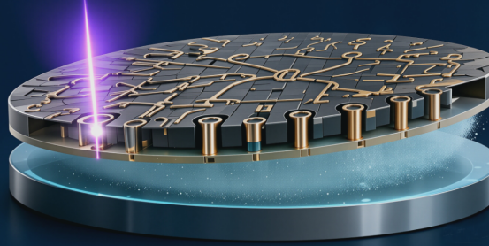
Ultrafast lasers have pulse widths as short as one-trillionth of a second or even less, injecting energy into materials in an extremely short time—faster than heat can diffuse to surrounding material. The material is removed before it can be "heated and conducted"—this is what the industry calls "cold processing": an extremely small heat-affected zone, extremely high processing precision, and almost no material limitations.
These characteristics happen to hit every pain point of advanced packaging: "high precision, low damage, hard and brittle materials." Here are several representative technologies as examples:
Ultrafast PCB Drilling: The Hammer of Thor for Breaking the "Compute Wall"
Process description: As AI servers, 5G communications, and IC substrates evolve toward high-density interconnects, traditional mechanical drilling is limited by tool wear and minimum hole diameter (>100μm), unable to meet the urgent demand of HDI and substrate-like PCBs for microvias (<50μm), high aspect ratios, and damage-free processing. Leveraging the "cold processing" characteristics of picosecond/femtosecond ultrafast lasers, energy instantly vaporizes material before heat conduction occurs, achieving precise removal and avoiding thermal melting and carbonization.
Laser requirements: As the material complexity of high-generation PCBs continues to increase, near-infrared femtosecond lasers with high energy (hundreds of μJ) and high repetition rates (MHz) are typically required.
Laser Stealth Dicing: Solving the Thinning Challenge Behind the "Memory Wall"
Process description: HBM requires stacking a dozen or more layers of DRAM dies, each of which must be thinned to an extremely low thickness. Ultra-thin wafers are highly prone to edge chipping and microcracks when cut with traditional blade dicing, directly threatening stacking yield. Laser stealth dicing focuses the laser inside the wafer, forming a modified layer along the dicing street, and then separates the dies through wafer expansion—no debris, extremely narrow kerf, and almost no chipping. It has become the mainstream solution for dicing ultra-thin wafers and MEMS devices.
Laser requirements: Nanosecond pulsed lasers with shaped beams in the 1099nm wavelength range are typically required.
Laser Debonding: The "Unsung Hero" Behind Multi-Layer Stacking for the "Memory Wall"
Process description: During thinning, ultra-thin wafers need to be temporarily bonded to a carrier wafer for support, and then separated after thinning is complete—this step is debonding. The laser passes through the transparent carrier and irradiates the bonding layer, modifying or decomposing it to achieve non-contact, low-stress separation, preventing damage to ultra-thin wafers during mechanical peeling. Depending on the bonding adhesive material used, the required laser wavelength varies slightly, and new processes are increasingly shifting toward ultrafast lasers. As packaging thicknesses continue to decrease, laser debonding is moving from "optional" to "mandatory."
Laser requirements: Depending on the bonding layer material used, laser selection ranges from ultraviolet to mid-infrared and far-infrared, typically requiring nanosecond or ultrafast pulsed lasers.
Laser Grooving: The "Pre-Process" for Cutting Low-k Materials Behind the "Memory Wall"
Process requirements: Advanced wafers are commonly covered with low-dielectric-constant (Low-k) materials, which are brittle and porous and highly prone to cracking and delamination when cut directly. Laser grooving first removes the Low-k layer along the dicing street, "clearing the path" for subsequent dicing, and is a standard process for ensuring dicing yield in advanced-node wafers. Depending on precision and heat-affected zone control requirements, laser source requirements range from ultraviolet nanosecond to picosecond and femtosecond.
Laser requirements: Depending on the material being processed and the required processing precision, laser grooving typically uses ultraviolet nanosecond, picosecond, or femtosecond lasers. As advanced packaging demand continues to grow, high-energy, long-lifetime ultraviolet femtosecond lasers are becoming the preferred choice for end customers.
TGV Glass Through-Vias: The Key Process for Breaking the "Interconnect Wall"
Process requirements: For glass substrates to handle vertical interconnects between chips, massive numbers of micron-scale through-holes must first be drilled in the glass—these are TGV (Through Glass Via) holes. High-energy femtosecond lasers in the 1-micron wavelength range can achieve high-aspect-ratio, smooth-walled, precisely positioned microvia processing through local modification combined with wet etching, or through direct ablation. The quality of each hole depends on the stability of single-pulse energy—this places extremely demanding requirements on laser pulse stability and is becoming a litmus test for the quality of high-end ultrafast lasers.
Laser Copper metal 3D Printing: A New Weapon for Breaking the "Thermal Wall"
Process requirements: Copper is the preferred material for heat dissipation structures, but it has high reflectivity for commonly used industrial laser wavelengths and conducts heat extremely quickly, making it a recognized difficult-to-process material. With the maturation of high-power green lasers, laser metal 3D printing is now achieving direct forming of complex copper heat dissipation structures—such as three-dimensional microchannel cold plates that cannot be manufactured by traditional processes, greatly improving heat exchange area and fluid design freedom, and providing next-generation thermal solutions for ultra-high-power-density chips.
Laser requirements: To meet processing efficiency and quality requirements, high-repetition-rate (tens of MHz), high-power (hundreds of watts), nanosecond quasi-continuous-wave green lasers are typically required, with very high power stability requirements (typically<2%).
As can be seen, ultrafast lasers are present at nearly every demolition site of the four walls. They do not produce computing power, but they are the "mother machine" for computing power evolution. They do not move data, but they determine how fine the substrates and stacks carrying data can be.
04
Looking Ahead: Domestic Opportunities in the AI Era
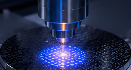
Looking at where we stand today, several trends are already quite clear:
First, demand continues to expand. Demand for AI compute is still growing rapidly, and advanced packaging capacity continues to expand. Technologies such as glass substrates, HBM, and chiplets are successively moving deeper into industrialization. As a core tool for precision processing of hard and brittle materials, ultrafast lasers are an indispensable link in this capacity expansion wave. According to a brokerage research report, the potential market for ultrafast laser equipment in scenarios such as glass interposers and glass carriers alone could reach the hundred-billion-yuan level (Source: Huatai Securities research report).
Second, the technology threshold keeps rising. Take TGV as an example: processing millions of through-vias places extremely stringent demands on the single-pulse energy stability of lasers. Industry analysis notes that under advanced processes, scenarios such as laser stealth dicing and debonding generally require pulse energy RMS fluctuation to be controlled within ±0.5%, and some scenarios are measured by even higher peak-to-peak stability metrics. Being able to “fire” is merely the passing line; “every shot being stable” is the ticket to entry.
Third, the window for domestic substitution has opened. For a long time, the high-end ultrafast laser market has been dominated by overseas brands, while the rise of China’s advanced packaging industrial chain has provided domestic lasers with their most valuable proving ground and iteration opportunities. Against the broader backdrop of domestic substitution in semiconductor equipment, self-reliance and controllability of core light sources have become an industry consensus—this is a rare historic window.
In AI’s next chapter, what’s at stake is not just how smart the algorithms are, but how much the physical foundation can carry.
The four walls will not disappear on their own, but someone needs the tools to tear them down.
And we believe laser technology is the best tool for the job.
 Order Frenzy: Laser Earnings Reveal 10B+ Backlogs — Who Wins?
 AI Compute Land Grab: What 30 Laser Earnings Reports Reveal
 Action-Cam Pioneer's Optical Pivot? GoPro to Sell Itself to Optics Firm for $285M
 Wuhan Team "Grows"Next-Gen Photovoltaic Film to Let Solar Panels Harvest More Sunlight
 Vietnam Plant + Europe Upgrade: Laser Leader Deepens Global Push
 Yang Gaojie, Rationalite Photonics: 3D Optical Computing to Break AI's Compute Wall
 Kingfit's Jin Songqing: Powering the Laser Industry Chain with Advanced Cooling Technology
 Laserion: Breaking Ultrafast Laser Bottlenecks to Industrialize Homegrown High-End Sources
 XTRI-tech's Yao Caihong: Building High-End Manufacturing
 Glitterin Tech's Three Photonic Pillars: Building the Optical Backbone of the AI Era