The "Light Chasers" in the Deep Ultraviolet World
source:China Science Daily
keywords:
Time:2025-12-09
Source: China Science Daily 30th Jul 2024
From the worship and utilization of light in primitive societies to the research and application of light in modern times, humanity’s history of "chasing light" has run through the entire course of civilization development.
The discovery that sunlight consists of seven colors, that radio waves can be used for communication, that ultraviolet light can sterilize, and that X-rays and gamma rays can penetrate the internal structure of objects... After the invention of lasers, the "light chasers" have explored wavelengths of light, shortening them from the visible spectrum (400 to over 700 nanometers) to ultraviolet light (over 300 nanometers).
As time entered the late 20th century, people set a new goal—to march into deep ultraviolet light with wavelengths shorter than 200 nanometers.
Unlike all previous chapters in the history of optics, this time, the "light chasers" leading the way are the Chinese.
Boldly Venturing into the "No-Man’s Land"
Deep ultraviolet lasers are characterized by short wavelengths, high energy resolution, and high photon flux density, making them highly valuable in fields such as laser lithography and laser micromachining. Some advanced scientific instruments also use them as "probes" to explore the internal structure of objects.
For a long time, the international laser community generally believed that 200 nanometers was an insurmountable barrier. Whoever could cross it and take the lead in developing practical, precision deep ultraviolet laser sources would seize the commanding heights in the deep ultraviolet field.
This challenge deeply attracted Chinese scientists. As early as 1990, Chen Chuangtian, a renowned Chinese artificial crystal expert, noticed the potassium fluoroberyllate borate (KBBF) crystal and its optical properties. In 1996, together with laser expert Xu Zuyan, he used a multi-wavelength, widely tunable optical parametric amplifier to generate 184.7-nanometer laser light for the first time, bringing hope for breaking the "curse" of 200 nanometers.
In 2001, Chen Chuangtian, who had transferred to the Technical Institute of Physics and Chemistry (TIPC), Chinese Academy of Sciences, led his team to successfully grow practical KBBF crystals—the world’s only nonlinear optical crystal capable of directly generating deep ultraviolet laser light through frequency doubling.
For his part, Xu Zuyan had, since the late 1980s, cherished the original aspiration of "filling the gap" and attempted to develop deep ultraviolet lasers.
Thus, Chen Chuangtian (master of crystal technology) and Xu Zuyan (master of laser technology) hit it off immediately and decided to join forces to venture into the "no-man’s land" of deep ultraviolet light.
Their first step was to find users with demands for deep ultraviolet lasers, based on which they would design and manufacture corresponding deep ultraviolet laser devices. To seek cooperative users, over the next three years, the over-60-year-old Xu Zuyan transformed into a "salesman," traveling to more than a dozen research institutions across the country to advocate passionately and elaborate on the potential of deep ultraviolet lasers in scientific research.
At that time, the question he was asked most frequently was: "What papers have been published overseas in this field? Are there any similar international cases?" Each time, Xu Zuyan replied truthfully: "At present, no one else in the world is engaged in this research—only we have published papers on it." Unsurprisingly, he always returned empty-handed.
Just as Xu Zuyan and Chen Chuangtian were at a loss, two emails brought a turning point.
The emails came from Zhou Xingjiang, a researcher at the Institute of Physics (IOP), Chinese Academy of Sciences, who had just returned from a visiting scholarship in the United States. Before his return, Zhou had worked at the Stanford Synchrotron Radiation Lightsource (SSRL) at Stanford University, researching the electronic states inside high-temperature superconducting materials. After coming back to China, he couldn’t find a suitable research platform for a time because there were no applicable synchrotron radiation light source facilities in the country back then.
One day in May 2004, Zhou Xingjiang accidentally came across a paper published by Chen Chuangtian and Xu Zuyan in an international journal. In the paper, they reported achieving 184.7-nanometer deep ultraviolet all-solid-state laser using the world’s first multi-wavelength, widely tunable optical parametric amplifier developed by Xu Zuyan. This sparked an idea in Zhou: "Could my research be realized with a deep ultraviolet laser?" Following the authors’ contact information in the paper, he sent an email to both Xu Zuyan and Chen Chuangtian, and soon received replies and an invitation. Thus, Zhou Xingjiang became their first cooperative user.
Supported by a special fund from the Ministry of Finance and the Chinese Academy of Sciences’ Instrument Development and Renovation Program, the collaboration achieved an initial success through the joint efforts of all parties. At the end of 2006, they developed the world’s first "vacuum ultraviolet laser angle-resolved photoemission spectrometer" using deep ultraviolet laser as the light source, and successfully measured the energy and momentum of electrons. Looking at the energy spectrum displayed on the computer, Zhou Xingjiang couldn’t contain his excitement: "Its precision is even higher than that of the photoemission spectrometer with the third-generation synchrotron radiation light source!"
Buoyed by this successful experience, Chen Chuangtian and Xu Zuyan gained greater confidence to move forward. In 2007, the Ministry of Finance and the Chinese Academy of Sciences jointly launched a pilot special program for "National Major Scientific Research Equipment Projects." "Development of Cutting-Edge Equipment for Deep Ultraviolet Solid-State Laser Sources" (hereinafter referred to as the Phase I Project) was selected as one of the first 8 pilot projects launched, with the goal of developing 8 types of practical and precision deep ultraviolet solid-state laser sources. Led by TIPC, the project appointed Xu Zuyan and Chen Chuangtian as chief scientists.


Deep Ultraviolet All-Solid-State Laser Photoemission Electron Microscope
Conquering the Practical-Grade KBBF Crystal
In the development of deep ultraviolet solid-state laser sources, the KBBF crystal marks the starting point of the R&D chain.
The KBBF crystal is like a tiny pebble with a small volume. Its layered structure is highly prone to cleavage, making it extremely difficult to grow large, thick crystals—naturally grown crystals are only 0.1 millimeters thick. To make things harder, KBBF crystal growth cannot adopt the traditional seed crystal method; it has to rely on spontaneous growth. Even if crystal "seeds" are sown, they cannot induce directional nucleation and growth on the substrate. Instead, nucleation occurs spontaneously at multiple sites, ultimately yielding a batch of small, thin crystal fragments.
In July 1999, Chen Chuangtian took the lead in setting up a research team, and Dr. Wang Xiaoyang, a researcher at TIPC, became one of its core members. He joined Chen’s team in 2004, taking charge of KBBF crystal growth.
KBBF crystal growth mainly adopted the "furnace swarm strategy": it takes four months to grow a single batch in one furnace. Therefore, the team set up a cluster of furnaces, each configured with distinct growth conditions.
Every furnace opening felt like unboxing a mystery box, and the results were always unsatisfactory.
Just as Wang Xiaoyang was feeling utterly frustrated, in the second half of 2006, one furnace "performed admirably" for two consecutive cycles, producing KBBF crystals as thick as 3 millimeters. "It fully meets practical application requirements!" Wang sighed with relief, believing he had solved the crystal growth challenge.

KBBF Family Crystals and Optical Contact Prism Coupling Devices
In 2005, the related technologies were filed for international patents and granted authorization. In 2020, the Ministry of Commerce and the Ministry of Science and Technology of China jointly issued a document, listing the "KBBF crystal growth and prism coupling device processing technology" in the restricted export technology catalogue. This has become one of China’s rare high-tech technologies subject to export control against foreign countries.
After the approval of the Phase I Project in 2007, the team continued to explore ways to develop deep ultraviolet prism-coupled frequency doubling devices into all-solid-state deep ultraviolet laser sources.
Dr. Zhang Shenjin, a researcher at TIPC, was one of the key participants in the development of the world’s first picosecond 175–210 nm widely tunable deep ultraviolet all-solid-state laser source. He recalled that the summer of 2010 was an extremely stressful period for the team.
This picosecond 175–210nm widely tunable deep ultraviolet all-solid-state laser source was an international innovation. It was required not only to develop a practical and precision prototype and integrate it with the photoemission spectrometer—a piece of cutting-edge equipment—but also to achieve stable operation for 24 hours a day, with continuous runtime of at least 7 days per startup.
To meet the beam pointing requirements of the photoemission spectrometer after wide wavelength tuning, Xu Zuyan and Zhang Shenjin jointly discussed the key technical issues and solutions for second harmonic generation (SHG) and fourth harmonic generation (FHG). They ultimately independently developed two core systems: a high-precision 350–420nm widely tunable reverse cascaded second harmonic generation system, and a high-precision 175–210nm widely tunable deep ultraviolet laser generation, shaping and quasi-automatic beam pointing control system. These systems fully satisfied the requirements of the complete equipment.
Beneficiaries
As crystal and laser technologies were conquered one by one, an increasing number of customized deep ultraviolet solid-state laser device platforms came into being.
Zhou Xingjiang still has vivid memories of the over-a-decade-long collaborative research drive.
After the initial successful cooperation between Zhou Xingjiang, Chen Chuangtian and Xu Zuyan in 2006, they continued their partnership in the Phase I Project. Among the 8 sets of scientific instruments developed under the Phase I Project, Zhou’s team was responsible for building two and a half of them.
The "half set" of equipment refers to the upgrading of the vacuum ultraviolet laser angle-resolved photoemission spectrometer that Zhou had co-developed earlier. The other two complete sets include a deep ultraviolet laser spin-resolved angle-resolved photoemission spectrometer and a deep ultraviolet laser angle-resolved photoemission spectrometer based on a time-of-flight energy analyzer.
Upon the conclusion of the Phase I Project, Zhou Xingjiang hoped to obtain a deep ultraviolet laser device equipped with an ultra-low temperature research environment, which would enable the observation of the electronic structure of superconducting materials under ultra-low temperature conditions. He thus participated in the Phase II Project.
After 8 years of efforts, Zhou Xingjiang’s team, together with Chen Chuangtian and Xu Zuyan’s teams, developed the world’s first deep ultraviolet laser photoemission spectrometer with large momentum and ultra-low temperature capabilities. This instrument not only set a record for ultra-low temperature operation at 0.8 Kelvin, but also boosted the photon energy up to 7.4 electron volts. Since then, researchers have finally been able to accurately "see" the microscopic electronic structure of superconducting materials, and explore the origin of the unique physical properties of advanced quantum materials such as superconductors and topological materials.

In September 2013, researchers operated the deep ultraviolet laser angle-resolved photoemission spectrometer based on a time-of-flight energy analyzer.
In September 2013, researchers operated the deep ultraviolet laser angle-resolved photoemission spectrometer based on a time-of-flight energy analyzer.
Since the start of their collaboration in 2004, Zhou Xingjiang—witness and participant in the development of China’s ultraviolet solid-state laser equipment—has reaped abundant rewards. In 2013, he was awarded the Asia Achievement Award of the Overseas Chinese Physics Association for his significant research outcomes achieved on the platform of deep ultraviolet all-solid-state laser cutting-edge devices. This year, based on the deep ultraviolet laser angle-resolved photoemission spectrometer with large momentum and ultra-low temperature capabilities, he revealed key information about the pairing mechanism of iron-based superconductors, attracting international attention.
Another beneficiary of deep ultraviolet solid-state laser devices is the Dalian Institute of Chemical Physics (DICP), Chinese Academy of Sciences. During the Phase I Deep Ultraviolet Project, the customized deep ultraviolet laser source developed by TIPC for DICP enabled the latter to discover many new phenomena, such as the regulatory effect of graphene on catalytic reactions and the confined enhancement effect of graphene on surface reactions catalyzed by platinum.


In September 2013, researchers were operating a deep ultraviolet laser photochemical reactor. Image courtesy of TIPC.
Forging Ahead into the Future
After 15 years of exploration through two phases of projects, China’s deep ultraviolet scientific research instruments have initially formed an independent innovation chain of "deep ultraviolet crystals–laser sources–cutting-edge equipment–scientific research–industrialization".
In terms of applications, the 84-year-old Xu Zuyan has a heartfelt aspiration—to use deep ultraviolet all-solid-state laser equipment to establish an international benchmark for length metrology. With the development of manufacturing, the requirements for measurement accuracy are constantly increasing. As early as the beginning of the 19th century, physicists proposed the idea of using visible light wavelengths as the length standard. Xu Zuyan hopes that the aluminum ion optical frequency standard equipment developed in the Phase II Project, leveraging high-precision deep ultraviolet lasers, will help China "establish its own national length standard and take the lead globally".
Today, the once virgin territory of deep ultraviolet lasers has blossomed into a flourishing landscape. Faced with boundless application possibilities, Xu Zuyan has repeatedly emphasized: "Breakthroughs in large-scale scientific instruments can never be the achievement of a single individual’s efforts. Instead, they are the fruits of collaborative efforts between the state, the Chinese Academy of Sciences, and various research institutions—they embody the crystallization of collective wisdom. No matter how the future unfolds, this fundamental truth will remain unchanged."
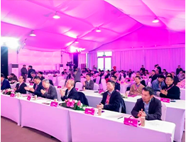 2026 China Laser Leadership Summit Opens in Shanghai, Leaders Talk Laser-Intelligence Integration
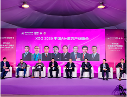 8 Laser Leaders Debate Laser-AI Integration & Two-Way Empowerment at Shanghai Summit
 10 New Laser Startups Emerge; Giants Like Han's Laser Nurture New Players for Future Race
 Lumentum Expands U.S. Chip Manufacturing to Supply AI Data Center Core Lasers
 Surges Sharply at Opening! Han's CNC Successfully Listed on the Hong Kong Stock Exchange
 Qiming Photonics: Nobel-Powered "Optical Engine" for the Computing Age
 Chen Kangkang of Anyang Laser: The "Hard Tech Long March" Behind a Single Optical Fiber
 Exclusive Interview with Academician Gu Bo: Escaping the Involution Trap in the Laser Industry
 Li Qi from Sichuang Laser: Pioneering High-Power Laser Tech for New Cross-Industry Use Cases
 Awardee Chen Weibiao Pushes Space Laser Tech to Build China's Aerospace Leadership