Anteland Chen Naiqi: 10-Yr Persist in Indep R&D of Laser Direct Writing, Serve Global Clients
source:Laser Manufacturer News
keywords:
Time:2025-09-17
Source: Laser Manufacturer News 1st Sep 2025
When a laser beam accurately outlines micron-level patterns on photosensitive materials, a "maskless laser direct writing revolution" in the manufacturing industry is quietly unfolding. Amid this wave of technological iteration, Shenzhen Anteland Image Technology Co., Ltd., with ten years of dedicated commitment, has grown from a new player in the industry when it was founded in 2015 to a current leader in laser direct writing technology—holding 50 invention patents and serving numerous customers worldwide.
Today, Shenzhen Anteland’s laser direct writing equipment has penetrated into the "capillaries" of the manufacturing industry: from the precision wiring of PCB (Printed Circuit Board) boards to the tiny pixels of LCD (Liquid Crystal Display) panels, and from the exquisite screen printing plate making for garment, packaging, glass, and ceramics—these "sculptors of light and shadow" are redefining the precision boundaries and efficiency limits of traditional manufacturing. More notably, its original patented DFAI (Digital Focus Array Imaging) technology has broken the technical barriers of the DMD solution developed by TI (Texas Instruments) of the US, setting new benchmarks in core indicators such as minimum line width, exposure power, and large-format efficiency. This achievement has enabled "Intelligent Manufacturing in China" laser equipment to secure industry-leading delivery volume and growth rate in the global market.
Recently, on the occasion of the 10th anniversary of Shenzhen Anteland Image Technology Co., Ltd., we at Laser Manufacturer News conducted an exclusive interview with Mr. Chen Naiqi, Chairman of Shenzhen Anteland. In this interview, Chairman Chen Naiqi will take us into the microcosmic world of laser direct writing, revealing how a technology moves from the laboratory to the production line, and from Chinese factories to workshops in Europe and the US. He will also discuss how maskless lithography is reshaping the future of manufacturing, and what new possibilities the intelligentization of laser equipment will open up under the wave of AI. This is not only the 10-year journey of a single enterprise, but also a vivid epitome of China's high-end manufacturing moving from "following" to "keeping pace" and then to "leading the way".

Mr. Chen Naiqi, Chairman of Shenzhen Anteland Image Technology Co., Ltd.
Laser Manufacturer News: As a leading domestic enterprise in R&D of laser direct imaging technology and complete equipment, what breakthrough progress has Shenzhen Anteland made in technological R&D and industrial application since its establishment in 2015?
Mr. Chen: The company was founded in 2015. It obtained the qualification certification of National High-Tech Enterprise in 2019, was awarded the title of "Shenzhen Specialized, Refined, Characteristic, and Innovative Small and Medium-sized Enterprise" in 2021, and won the title of "Little Giant" Enterprise (a national-level recognition for specialized, refined, characteristic, and innovative enterprises) awarded by the Ministry of Industry and Information Technology of the PRC in 2023.
The company focuses on the R&D of core laser direct writing technologies, as well as the development, production, and sales of complete equipment. Since its establishment, it has maintained high investment in R&D. Through independent R&D, it has achieved breakthroughs in the entire technology chain of laser direct writing equipment manufacturing, covering "core technologies + key processes + core components + complete equipment". In 2023, its technological achievements passed the evaluation of an expert group, which confirmed that the company’s technologies are at the leading level in China.
To improve the image precision of laser direct writing, the company has successfully developed an optical system suitable for large-depth-of-field digital focusing and a high-precision assembly process, realizing precise shaping and high-power focusing of laser beams. This has solved the industry’s long-standing challenges of "micron-level large aspect ratio exposure" and "difficult penetration of thick films of photosensitive materials".
By independently developing a dual-closed-loop high-speed motion control algorithm and a real-time exposure image compensation algorithm, and adopting the method of multi-beam laser parallel high-speed scanning exposure, the company has overcome the problem that "large-format efficiency fails to meet production needs".
At present, the company has formed a product line for mass sales, mainly including high-precision laser direct writing exposure machines for polyester mesh and steel wire mesh. Positioned in the mid-upstream of the manufacturing industry, its products serve numerous downstream manufacturing customers, covering vertical fields such as PCB (Printed Circuit Board), LCD (Liquid Crystal Display), optoelectronic display panels, as well as consumer goods manufacturing (e.g., garments, ceramics, high-end printing and packaging).
Since its establishment, the company has established a product and market strategy centered on serving global customers. All its product series have obtained EU CE safety certification. Currently, 50% of its customers are manufacturing enterprises from Europe and the US, 40% from China, and 10% from Southeast Asia. In the screen printing plate making link, which is essential for industrial manufacturing, the delivery quantity and growth rate of its laser equipment have ranked among the industry’s leading positions.
Laser Manufacturer News: Could you elaborate on the maskless lithography technology based on the core technology of DFAI (Digital Focus Array Imaging)? What are its unique advantages compared with traditional technologies and other similar technologies?
Mr. Chen: There are two methods to achieve high-precision image writing: masked and maskless. The widely used film exposure, chrome plate exposure, and the current most advanced semiconductor lithography processes belong to masked lithography. Electron beam lithography, which is used to make IC (Integrated Circuit) photomasks, falls into the category of maskless lithography.
Laser direct writing is a type of "maskless lithography" technology. Its core technical principle is to use computer control to make a laser beam directly write the required image on photosensitive materials. This eliminates the time and cost of manufacturing photomasks. Theoretically, by detecting the micro-deformation of the exposed material and adjusting image data in real time, it can achieve more precise alignment and size matching.
Benefiting from the continuous improvement of laser technology, computing capabilities, and precision manufacturing capabilities, laser direct writing technology is also advancing rapidly in terms of precision and efficiency. Currently, in the manufacturing process of electronic products and consumer goods, replacing traditional film exposure with laser direct writing has become one of the key contents of process upgrading. In the higher-precision pan-semiconductor lithography field (e.g., advanced packaging, MEMS (Micro-Electro-Mechanical Systems), optoelectronic chips, biochips), the industry is actively exploring the replacement of photomask exposure processes with laser direct writing.
Before the establishment of Shenzhen Anteland, the mainstream laser direct writing technology solution in the market was the DMD (Digital Micromirror Device) digital mask exposure solution, whose core technologies and chips were controlled by Texas Instruments (TI) of the US. Through research, analysis, and comparison of various technical routes, Shenzhen Anteland independently developed the "DFAI (Digital Focus Array Imaging)" technology solution, which is different from the DMD solution. This technical solution is more conducive to meeting the requirements for exposure precision, exposure energy, and exposure efficiency in more application scenarios.
The company has carried out collaborative R&D in technical fields such as "optics + mechanics + electronics + software algorithms", achieving breakthroughs in indicators including minimum line width, exposure power range, large aspect ratio 3D imaging, and large-format exposure efficiency. based on R&D achievements at different technical levels, the company’s product team conducts industrialization R&D and launches a series of equipment models to meet the needs of customers in vertical fields. These products have replaced foreign同类 key components and complete equipment, realizing full independent guarantee and reaching the industry-leading level.
Laser Manufacturer News: Currently, which fields are the company’s laser direct writing plate making equipment mainly applied in? Could you share some cooperation cases with benchmark customers? What are the key factors that make these customers choose Shenzhen Anteland?
Mr. Chen: At present, the company’s mass-produced laser direct writing plate making equipment is suitable for various manufacturing customers who have plate making needs for polyester mesh and high-precision steel wire mesh.
We internally classify customer needs into two categories: industrial and consumer. Industrial customers mainly include enterprises engaged in PCB manufacturing, LCD manufacturing, and display panel manufacturing; consumer customers mainly cover industries such as garments, ceramics, glass, and printing and packaging.
When it comes to case sharing, people may focus more on the industrial product manufacturing field. However, we have observed an interesting field—the garment industry. It seems like a very traditional industry, and we once thought it was far from technological progress. But after engaging with it, we found that the industry has an urgent demand for improving traditional processes. Our equipment was quickly verified: by replacing traditional film exposure equipment, it eliminates the cost and pollution of film manufacturing, and shortens the plate making time from several hours to 2 minutes. Moreover, compared with imported similar equipment from European manufacturers, our equipment maintains overall leading advantages in efficiency, precision, format, and photosensitive material compatibility. Therefore, currently, all leading large-scale garment OEM (Original Equipment Manufacturer) enterprises in China have basically adopted our equipment.
Laser Manufacturer News: The company currently holds a number of patents, including the laser direct writing imaging control method. What are the key directions of R&D in the future? Will you expand into other laser application fields?
Mr. Chen: The company positions itself as a technology-driven enterprise. Therefore, we have always maintained a relatively high proportion of R&D investment and actively laid out patents around our independently developed DFAI laser direct writing imaging technology. Up to now, the company has obtained 50 authorized invention patents and 34 authorized software copyrights, with more than 200 patents under application.
The company’s patent applications are closely focused on fields directly related to laser direct writing imaging, such as optics, image processing, motion control, and detection methods.
The company’s current main R&D direction is high-speed maskless lithography and detection technology at the micron and sub-micron levels. We will always focus on technologies and products related to high-precision imaging, and there are no plans to enter other laser application fields at present.
Laser Manufacturer News: With the continuous development of science and technology, in your opinion, what new application expansion directions will laser direct writing imaging technology have in fields such as industrial manufacturing and semiconductors in the future?
Mr. Chen: High-precision imaging is the foundation of all high-end manufacturing. Applying laser direct writing technology to a wider range of manufacturing fields has always been our core work goal.
In our understanding, currently, in the range of 30-100 microns line width precision, laser direct writing imaging equipment can fully replace the traditional masked imaging process. In the near future, for precision ranging from 3 microns to 0.35 microns—especially for large-format manufacturing needs (e.g., optoelectronic displays, advanced packaging)—the precision and production efficiency of laser direct writing equipment will also be able to meet customers’ mass production needs. This will bring the advantages of maskless lithography (such as flexibility, low cost, and higher compatibility) to customers in the industry.
As for the cutting-edge lithography below 10 nanometers, which has attracted social attention, the future application of laser direct writing will likely be more in the scientific research field where the requirement for mass production efficiency is not high.
Laser Manufacturer News: Currently, the industry pays great attention to the development trend of intelligence and integration of laser technology. What explorations and practices has Shenzhen Anteland made in this regard? How to integrate new technologies such as AI into laser equipment to improve the equipment’s intelligence level and production efficiency?
Mr. Chen: As a technology-driven company, we pay close attention to the development and application of AI technology, and we are also shocked and inspired by the rapid progress of large model technology.
At present, our practices in AI mainly cover two aspects: on the one hand, we use AI—especially LLM (Large Language Model) technology—to optimize our R&D process, including practices such as AI coding and AI participating in hardware scheme selection and technical review.
On the other hand, we have been committed to integrating AI algorithms and data that can be directly combined with products (such as image processing algorithms, precision compensation deep learning algorithms, and equipment fault prediction algorithms) into our products, so as to better serve our customers.
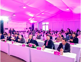 2026 China Laser Leadership Summit Opens in Shanghai, Leaders Talk Laser-Intelligence Integration
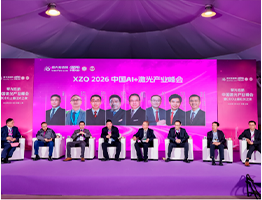 8 Laser Leaders Debate Laser-AI Integration & Two-Way Empowerment at Shanghai Summit
 10 New Laser Startups Emerge; Giants Like Han's Laser Nurture New Players for Future Race
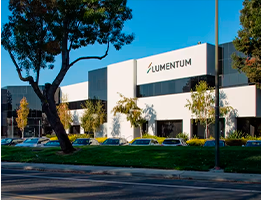 Lumentum Expands U.S. Chip Manufacturing to Supply AI Data Center Core Lasers
 Surges Sharply at Opening! Han's CNC Successfully Listed on the Hong Kong Stock Exchange
 Qiming Photonics: Nobel-Powered "Optical Engine" for the Computing Age
 Chen Kangkang of Anyang Laser: The "Hard Tech Long March" Behind a Single Optical Fiber
 Exclusive Interview with Academician Gu Bo: Escaping the Involution Trap in the Laser Industry
 Li Qi from Sichuang Laser: Pioneering High-Power Laser Tech for New Cross-Industry Use Cases
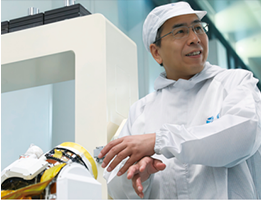 Awardee Chen Weibiao Pushes Space Laser Tech to Build China's Aerospace Leadership