ESI Unveils Innovative Solution for Laser Processing of Thin Silicon Wafers
source:ESI
release:Johnny Lee
keywords: laser HAZ ESI micromachining semiconductor
Time:2015-09-30
The UltrusTM system combines ultrafast high-pulse-rate lasers and ESI's proprietary beam positioning technology to provide a high-throughput, high-accuracy grooving solution that addresses the challenges associated with processing thinner and more fragile materials. Since the UltrusTM system allows for higher die break strength (DBS) and a smaller heat affected zone (HAZ), semiconductor manufacturers can now process newer thin wafers efficiently at the higher level of accuracy required and low-k materials—as well as current materials—without risking damage to the underlying devices.
"For semiconductor manufacturers, just keeping pace with Moore's Law requires constant innovation across their processing operations," said
Although laser-based platforms have become essential for cost-effective wafer processing, the adoption of more fragile materials has presented semiconductor manufacturers with processing challenges related to maintaining high throughput at high accuracy while minimizing the risk of damage to the material—and thereby decreasing yields. Using ultrafast, high-pulse-rate laser technology to precisely remove metal layers and fragile materials allows for higher die break strength and smaller heat affected zones, leading to higher yields and a lower total cost of ownership.
Availability
The UltrusTM laser system is available now worldwide. For more information go to: http://www.esi.com/Products/Semiconductor/LaserScribingGrooving/Ultrus.aspx.
about ESI
ESI's integrated solutions allow industrial designers and process engineers to control the power of laser light to transform materials in ways that differentiate their consumer electronics, wearable devices, semiconductor circuits and high-precision components for market advantage. ESI's laser-based manufacturing solutions feature the micro-machining industry's highest precision and speed, and target the lowest total cost of ownership. ESI is headquartered in
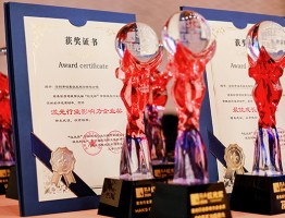 56 Benchmarks Honored: 9th Secret Light Awards Highlights China Laser Chain Innovation
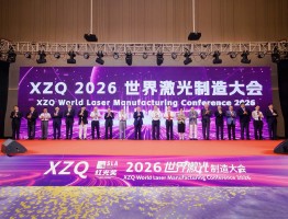 Laser Intelligence, Photonics Future: XZQ 2026 WLMC Concludes Successfully
 Laser Giants' AI Bet: Decoding Earnings to Find the Next Winner
 Orders Reign Supreme: Laser Firms' Battle—$10B Backlogs vs. Overseas Breakouts
 Q1 Earnings Released: A Tale of Two Strategies Among the World's Four Largest Laser Companies
 HSG Laser's He Hongming: Innovation Drives Laser Manufacturing Future
 Xi Jingyu from Mingyu Technology: Carving the Future of Hometown Industries with Laser
 Qiming Photonics: Nobel-Powered "Optical Engine" for the Computing Age
 Chen Kangkang of Anyang Laser: The "Hard Tech Long March" Behind a Single Optical Fiber
 Exclusive Interview with Academician Gu Bo: Escaping the Involution Trap in the Laser Industry