
All-Si Laser With High Optical Gains Could Advance Integrated Photonics
source:
keywords: All-Si Laser integrated silicon photonics optically pumped
Time:2018-01-23
SHANGHAI, Jan. 22, 2018 — An optically pumped, all-silicon (Si) distributed feedback laser has been demonstrated. Researchers used active layers of high-density Si nanocrystals to develop the laser. The new laser provides high optical gains, overcoming the low efficiency that has been historically exhibited in Si emission.
To enhance Si emission intensity, researchers from Fudan University developed a film growth technique for high-density Si nanocrystals. They then designed and fabricated a DFB resonance cavity using these high-gain Si nanocrystals. The lasing emission was observed by optical pumping with femtosecond pulses.
The researchers used a high-pressure, low-temperature passivation approach. They found that, compared with normal-pressure hydrogen passivation at higher temperatures (greater than 500 degrees Celsius), a prolonged high-pressure passivation at relatively low temperatures contributed a full saturation of dangling bonds. This led to optical gains comparable to those achieved by gallium arsenide (GaAs) and indium phosphide (InP).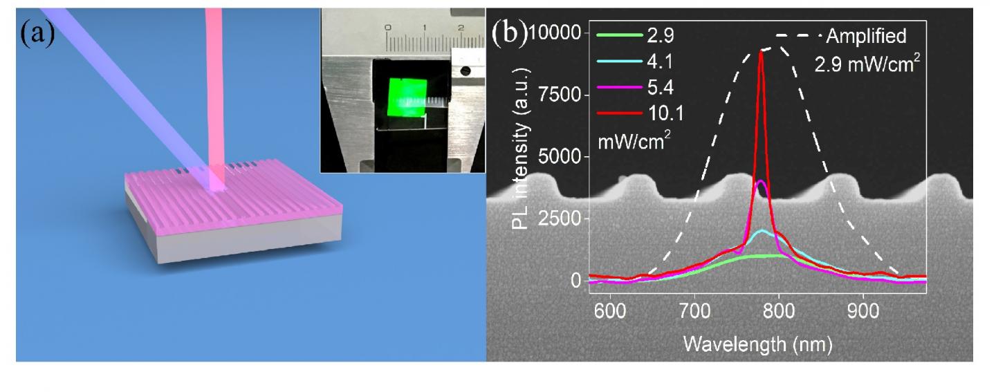
A schematic image of the DFB Si laser (a). A photograph of a fabricated DFB device (Inset). Emission spectra of the Si laser as a function of pump power (b). A cross-sectional SEM image of the DFB structure (background).
The Si nanocrystal-embedded layer (Si NC layer) was prepared on a fused quartz substrate. The gain of the Si NC layer was measured by means of variable stripe length. To correct the measured gain, optical loss was acquired by means of a shifting excitation spot technique.
The laser showed reliable repeatability. The lasing peaks of the four samples made under similar fabrication conditions were within the spectral range of 760 to 770 nm. The team said that the variation in the lasing peak was due to the slight difference in effective refractive indices. The full width half maximum of the emission peak was narrowed from about 120 nm to 7 nm when the laser was pumped above threshold.
According to the researchers, theirs is the world’s first all-Si laser. This optically pumped all-Si laser could lead to the realization of an electrically pumped all-Si laser for integrating microelectronics and optoelectronics, thus enabling integrated silicon photonics.
 Five Laser Firms See Executive Reshuffles: Younger Leaders Take the Helm
 30+ Laser Startups Storm 2026: Who's Positioning for the Future?
 Three Chinese Laser Makers Expand Into South Korea: Raycus, YIFI and Strong Laser
 Hyperline Debuts at ESSEN 2026 with Premium Laser Welding Solutions
 56 Benchmarks Honored: 9th Secret Light Awards Highlights China Laser Chain Innovation
 Glitterin Tech's Three Photonic Pillars: Building the Optical Backbone of the AI Era
 A Female Pioneer's 20-Year Quest for World-Leading Laser Thin Film Breakthroughs
 HSG Laser's He Hongming: Innovation Drives Laser Manufacturing Future
 Xi Jingyu from Mingyu Technology: Carving the Future of Hometown Industries with Laser
 Qiming Photonics: Nobel-Powered "Optical Engine" for the Computing Age