
From Sand to Silicon: How Impressive Is Laser Ball Attach Technology?
source:VI Laser
keywords:
Time:2026-08-25
Source: VI Laser 6th Aug 2026
In an era of rapid technological change, chips are hailed as the “staple food” of modern industry—the core engine driving smartphones, artificial intelligence, data centers, and even new energy vehicles. Yet a powerful chip is not born solely under precision lithography machines. Between a pristine silicon wafer and the integrated circuits that end up in high-tech products lies a crucial, highly sophisticated step: packaging.
Among the many advanced packaging technologies, laser solder ball bonding is playing an increasingly critical role thanks to its high precision and efficiency. Today, let’s take a deep dive into the full journey of a chip—from wafer fabrication to laser solder ball bonding, and on to its vast application potential.
From Sand to Wafer: The Foundation of Chip Manufacturing
The journey of a chip begins with seemingly ordinary quartz sand. Through complex chemical purification, the quartz sand is transformed into electronic-grade polysilicon with a purity of up to 99.999999999% (eleven nines)—one of the purest solid materials that humans can mass-produce.
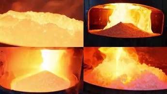
Next, this high-purity polysilicon is drawn into flawless cylindrical monocrystalline silicon ingots in crystal pulling furnaces using methods such as the Czochralski (CZ) or float zone (FZ) techniques. After slicing, grinding, and chemical mechanical polishing (CMP), the ingots become thin, uniformly thick slices with atomically flat surfaces—what we commonly call wafers. The mainstream wafer size in the industry has now reached 12 inches (300 mm).
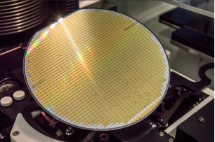
On the wafer, hundreds of complex processes such as lithography, etching, thin-film deposition, and ion implantation are used to “carve” billions of transistors, forming intricate integrated circuits. once all front-end processes are complete, the wafer is covered with densely packed chip units known as bare dice. At this stage, the bare die is extremely fragile—unable to connect directly with external circuits or withstand the external environment—making packaging absolutely essential.
Advanced Packaging: Key to Extending Moore's Law
Traditional packaging technologies, such as DIP (dual in-line package) and QFP (quad flat package), primarily connect chips to circuit boards through pins. However, as electronic products rapidly trend toward miniaturization, higher performance, and lower power consumption, traditional packaging is gradually hitting its limits in size, performance, and integration.
To extend Moore's Law, the industry has turned its attention to "advanced packaging." Unlike the traditional flow of cutting the wafer first and then packaging, advanced packaging approaches—such as wafer-level packaging (WLP)—typically complete packaging and testing on the entire wafer before dicing. This allows the package size to be nearly as large as the chip itself, greatly saving space.
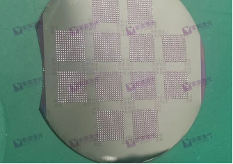
Among the many advanced packaging technologies, flip-chip technology represents a revolutionary breakthrough. It abandons conventional wire bonding and instead flips the chip over, using bumps on the chip surface to establish direct electrical connections with the substrate. This approach not only significantly shortens signal transmission paths and improves electrical performance and heat dissipation, but also creates conditions for achieving higher-density I/O (input/output) interfaces.
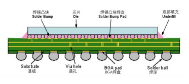
Laser Solder Ball Bonding: Precision "Welding" at the Micron Level
The core of flip-chip technology lies in how to precisely and efficiently create thousands of solder balls of consistent size on the chip's tiny pads. This is exactly where laser solder ball bonding comes into its own.
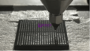
As the name suggests, laser solder ball bonding is an advanced process that uses laser energy to place solder balls. Its basic process can be summarized as follows:
1. Positioning: A high-precision CCD vision system rapidly scans and identifies the exact coordinates of each pad on the chip, automatically compensating for minor material deformation, with alignment accuracy up to ±5 μm (Zichen Laser's micro-ball machine can achieve ±2 μm).
2. Laser melting: A high-energy fiber laser (wavelength about 1064 nm) is precisely focused on a solder wire or tiny solder ball, melting it instantaneously (within milliseconds) to form a molten solder droplet.
3. Ball placement: Under the protection of high-purity nitrogen, the molten solder droplet is precisely jetted onto the target pad. The nitrogen prevents oxidation of the high-temperature solder ball in air, ensuring soldering quality.
4. Cooling and solidification: After contacting the pad, the solder cools rapidly and solidifies into a perfect spherical bump, completing the solder ball placement on the entire board.
Compared with traditional ball placement methods, laser solder ball bonding offers significant advantages:
Ultra-high precision: It can handle pads with extremely small pitch, meeting the high-density interconnect requirements of advanced-node chips, with solder ball coplanarity controllable at the micron level.
Non-contact processing: Laser processing does not cause mechanical stress damage to fragile chips, improving production yield.
No flux, no residue: The entire process requires no flux, eliminating the need for subsequent complex cleaning steps and removing the risk of contamination.
2.5/3D ball placement: It can easily handle 50 μm micro-bumps, meeting the demands of cutting-edge packaging such as 2.5/3D stacking and HBM (high-bandwidth memory).
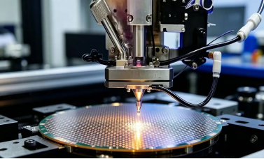
It can be said that laser solder ball bonding is the foundation for achieving more complex 3D integration technologies such as 2.5D/3D packaging and system-in-package (SiP). It is like installing precise "neural network endings" on the chip, enabling high-speed, stable information exchange with the outside world.
From Packaging to Application: Powering the Future of Technology
Chips processed with advanced packaging technologies such as laser solder ball bonding have their full performance potential unleashed, finding widespread application across nearly every aspect of modern life:
1. Artificial Intelligence and High-Performance Computing
AI accelerator cards and GPUs demand extremely high data transfer bandwidth and computing power. Chips built with 2.5D/3D packaging and laser solder ball bonding can integrate processors, high-bandwidth memory (HBM), and other components into a single package, dramatically reducing data exchange latency. They have become the core driving force behind AI large-model training and inference.
2. 5G Communications and the Internet of Things
5G base stations and IoT devices impose stringent requirements on chip size, power consumption, and RF performance. Technologies such as wafer-level packaging (WLP) and fan-out packaging make chips smaller, thinner, and more capable, perfectly matching the demands of mobile communications and ubiquitous connectivity.
3. Autonomous Driving and Automotive Electronics
Modern vehicles have effectively become “data centers on wheels.” From perception and decision-making to execution, autonomous driving relies on a vast number of highly reliable chips. Advanced packaging not only boosts computing capability but also enhances heat dissipation and reliability in demanding automotive environments.
Conclusion
In short, chip manufacturing is a grand engineering endeavor that brings together humanity’s finest intellect. If wafer fabrication constructs a microscopic world within tiny dimensions, then packaging technology—especially advanced processes such as laser solder ball bonding—builds the bridge connecting that microscopic world to macroscopic applications. As technology continues to evolve, the importance of the packaging stage will only grow, injecting sustained momentum into the future of technology.
 Order Frenzy: Laser Earnings Reveal 10B+ Backlogs — Who Wins?
 AI Compute Land Grab: What 30 Laser Earnings Reports Reveal
 Action-Cam Pioneer's Optical Pivot? GoPro to Sell Itself to Optics Firm for $285M
 Wuhan Team "Grows"Next-Gen Photovoltaic Film to Let Solar Panels Harvest More Sunlight
 Vietnam Plant + Europe Upgrade: Laser Leader Deepens Global Push
 Yang Gaojie, Rationalite Photonics: 3D Optical Computing to Break AI's Compute Wall
 Kingfit's Jin Songqing: Powering the Laser Industry Chain with Advanced Cooling Technology
 Laserion: Breaking Ultrafast Laser Bottlenecks to Industrialize Homegrown High-End Sources
 XTRI-tech's Yao Caihong: Building High-End Manufacturing
 Glitterin Tech's Three Photonic Pillars: Building the Optical Backbone of the AI Era