High-Efficiency Conversion Feeds R&D! Optoelectronic HOPE Model Builds a New Industrial Engine
source:China Intellectual Property Ne
keywords:
Time:2026-01-22
In the 11th lunar month, Changchun City, Jilin Province, located in the heart of the Northeast China Plain, was covered in a vast expanse of white snow, presenting a desolate yet magnificent scene. In an assembly and adjustment laboratory for large-aperture silicon carbide mirrors at the Changchun Institute of Optics, Fine Mechanics and Physics (CIOMP), Chinese Academy of Sciences (hereinafter referred to as CIOMP), researchers were monitoring the real-time updates of relevant laboratory data.
"In recent years, we have adhered to the development philosophy of integrating industry, academia, and research. Focusing on the technological heights of the optoelectronic field, we have accelerated the breakthrough of the 'bottleneck' problems in the manufacturing of high-end domestic equipment. Through high-quality creation, high-standard management, and high-efficiency transformation, we have promoted the application of patented technologies, achieved independent control of core equipment, and empowered the high-quality development of related industries," introduced Sun Shouhong, Deputy Director of CIOMP, to reporters.
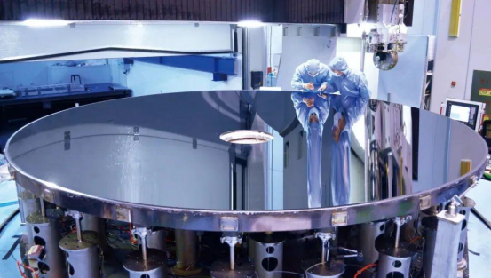
A Finished 4m Silicon Carbide Mirror (Photo courtesy of CIOMP)
The preparation of large-aperture silicon carbide mirrors is a core technology for large-scale optoelectronic imaging systems such as high-resolution earth observation, deep space exploration, and astronomical observation. It is crucial for enhancing China's optical system manufacturing capabilities and achieving leapfrog upgrades in large-aperture optoelectronic equipment. In recent years, CIOMP has actively carried out patent information mining and classified hierarchical management, supporting research teams to continuously break through multiple "bottleneck" technologies in the field of large-aperture silicon carbide mirror preparation. It has laid out more than 200 domestic and foreign invention patents and a number of technical secrets around the entire industrial chain manufacturing processes and equipment. Through patent transformation, it has incubated a number of industrial entities, forming an integrated intellectual property strategy layout for protection and application.
Closely focusing on the needs of the optoelectronic industry, starting from the application requirements of CMOS (Complementary metal-Oxide-Semiconductor) image sensor system integration, CIOMP has comprehensively laid out technical research directions such as design, manufacturing, and packaging. It has focused on the technology of front-illuminated image sensor process production lines, conducting patent layout from multiple dimensions including CMOS devices, through-silicon vias, wafers and semiconductor processing, and defect detection. "Driven by patented technologies, through the industry-academia-research collaboration model, we have joined hands with state-owned investment platforms and industrial chain enterprises to accelerate the industrialization of front-illuminated CMOS image sensor patented technologies. At present, we have built a production line with an annual output of 20,000 wafers, effectively realizing the domestic substitution of high-end CMOS image sensors. Relevant experiences have also been selected as excellent national and provincial cases of patent transformation and application," said Sun Shouhong.
Reporters learned that CIOMP has established an independent intellectual property management department, organically integrating intellectual property with project management and achievement transformation management, forming a standardized, systematic, and efficient scientific research management model centered on intellectual property rights, and continuously consolidating the foundation for the high-efficiency transformation and application of scientific research achievements.
Utilizing intellectual property rights in the field of high-precision objective lens technology, it has jointly developed high-throughput gene sequencer products with BGI Shenzhen, breaking two world records in sequencing throughput and sequencing cost; built a national-level Category A technology business incubator, cultivating 52 "Changguang series" enterprises, accelerating the value realization of intellectual property rights through enterprise operations; since 2015, it has achieved 3.5 billion yuan in revenue through the implementation of 348 intellectual property rights, rewarding 838 scientific researchers with a total of 1.68 billion yuan and their research teams with 760 million yuan... With patent transformation and application as the main theme, CIOMP has continuously built a full industrial chain patent transformation and application platform, established new disciplinary directions, used transformation income to further "feed back" scientific and technological research and development, and fully supported the high-quality development of the industry.
 2026 China Laser Leadership Summit Opens in Shanghai, Leaders Talk Laser-Intelligence Integration
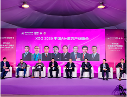 8 Laser Leaders Debate Laser-AI Integration & Two-Way Empowerment at Shanghai Summit
 10 New Laser Startups Emerge; Giants Like Han's Laser Nurture New Players for Future Race
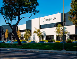 Lumentum Expands U.S. Chip Manufacturing to Supply AI Data Center Core Lasers
 Surges Sharply at Opening! Han's CNC Successfully Listed on the Hong Kong Stock Exchange
 Qiming Photonics: Nobel-Powered "Optical Engine" for the Computing Age
 Chen Kangkang of Anyang Laser: The "Hard Tech Long March" Behind a Single Optical Fiber
 Exclusive Interview with Academician Gu Bo: Escaping the Involution Trap in the Laser Industry
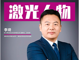 Li Qi from Sichuang Laser: Pioneering High-Power Laser Tech for New Cross-Industry Use Cases
 Awardee Chen Weibiao Pushes Space Laser Tech to Build China's Aerospace Leadership