Significant Progress Achieved in China's Laser Crystal Material Preparation
source:Guangdong Academy of Sciences,
keywords:
Time:2025-11-04
Source: Guangdong Academy of Sciences, Institute of Semiconductors, Optoelectronic Technology Center 3rd Nov 2025
Recently, the Optoelectronics Technology Center of the Institute of Semiconductors, Guangdong Academy of Sciences, has made significant progress in the preparation of laser crystal materials. Using a resistance furnace, it has successfully grown larger-sized Ce,Nd:YAG crystals, increasing the crystal diameter from the previous 40 mm to approximately 60 mm, with the crystal exhibiting uniform and stable optical properties.

YAG crystal: The "heart" of the laser
YAG crystals, particularly neodymium-doped (Nd:YAG) and cerium-neodymium co-doped (Ce,Nd:YAG) variants, can be regarded as the "heart" of many laser devices. They generate high-quality, high-power lasers, finding extensive applications in key national sectors such as optical communications, medical equipment, precision measurement, mechanical processing, and radar—playing a vital role in both our daily lives and cutting-edge technology.
Traditional Growth Methods: High Quality but High Cost
In the past, high-quality YAG crystals were mostly grown using induction furnace methods. While this approach yields crystals with excellent optical performance, it has significant drawbacks: it requires expensive iridium crucibles, and growing a single crystal takes over 30 days, resulting in extremely high production costs.
Resistance Furnace Method: Great Potential but Bottlenecks
In contrast, crystal growth using resistance furnaces shortens the cycle to around 7 days and reduces costs. However, due to slow technological development and external technological blockades, this process has long faced a bottleneck—the diameter of grown crystals has mostly remained around 40 millimeters. Smaller sizes mean fewer usable components per crystal and low material utilization, which has largely restricted its industrial application.
New Breakthrough: Larger, More Uniform, and More Efficient
To address this challenge, the research team at the Optoelectronics Technology Center, through dedicated research, comprehensively optimized and innovated everything from raw material ratios and temperature field structures to growth processes. They successfully increased the diameter of Ce,Nd:YAG crystals grown via resistance furnaces to approximately 60 millimeters, achieving a new breakthrough in crystal size under this domestic technical route.

This technological breakthrough has provided solid support for the large-scale industrialization of high-performance laser crystals and laid a technological foundation for the subsequent research and development of multi-functional doped crystals. This progress has not only broken the long-term size bottleneck that constrained the development of the resistance furnace method but also redefined the balance between crystal growth efficiency and cost control.
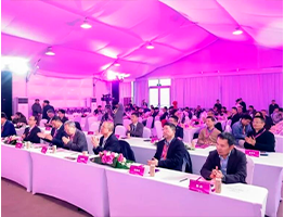 2026 China Laser Leadership Summit Opens in Shanghai, Leaders Talk Laser-Intelligence Integration
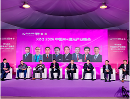 8 Laser Leaders Debate Laser-AI Integration & Two-Way Empowerment at Shanghai Summit
 10 New Laser Startups Emerge; Giants Like Han's Laser Nurture New Players for Future Race
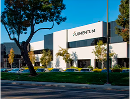 Lumentum Expands U.S. Chip Manufacturing to Supply AI Data Center Core Lasers
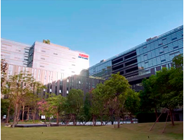 Surges Sharply at Opening! Han's CNC Successfully Listed on the Hong Kong Stock Exchange
 Qiming Photonics: Nobel-Powered "Optical Engine" for the Computing Age
 Chen Kangkang of Anyang Laser: The "Hard Tech Long March" Behind a Single Optical Fiber
 Exclusive Interview with Academician Gu Bo: Escaping the Involution Trap in the Laser Industry
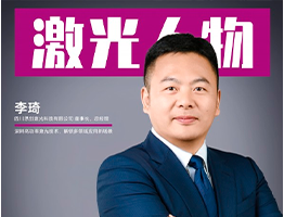 Li Qi from Sichuang Laser: Pioneering High-Power Laser Tech for New Cross-Industry Use Cases
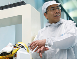 Awardee Chen Weibiao Pushes Space Laser Tech to Build China's Aerospace Leadership