
Organic photodetectors and plastic image sensors
source:Laser Manufacture News
release:Johnny Lee
keywords: ISORG Organic photodetectors
Time:2015-12-16
Laurent Jamet, ISORG, Co-founder & Director Business Development, laurent.jamet@isorg.fr
Thanks to important R&D activities started in years 2000 by the organic chemistry for organic photovoltaics, new semiconductor polymer materials were developed to convert light into electrical current. These materials were reused and modified (to extend their operation to visible and near infra-red spectrum with wide dynamic range) for development of optical sensors and serve the new industry of printed electronics.
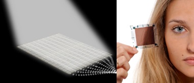
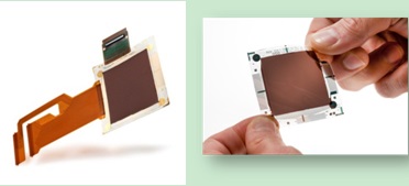
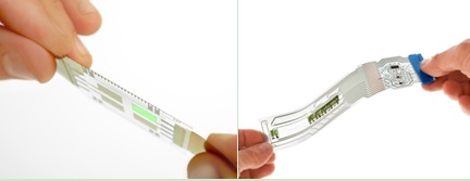
ISORG, the pioneer company in optical sensors in organic electronics, developed in collaboration with FlexEnable the first image sensor on plastic in the world, 1 million pixels, 85um pixel size.
Technology overview :
The technology of printed electronics is also called organic electronics, plastic electronics, large area electronics, flexible electronics depending on different considerations :
Organic Electronics comes from the materials used for manufacturing the device : conductive and transparent materials such ITO (Indium Titatium Oxide), semiconductor polymer materials (derivated from P3HT and Fullerene materials).
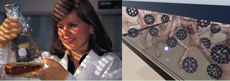
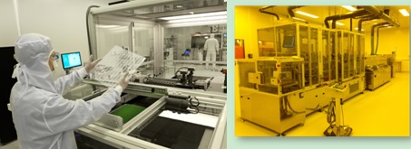
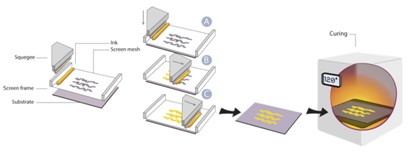
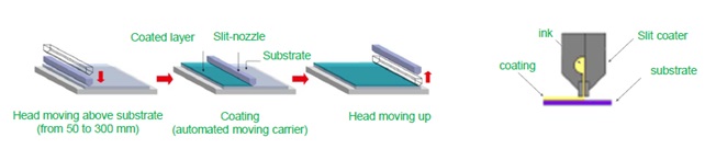
Printed Electronics comes from the manufacturing process : conductive and semiconductor materials are liquid and deposited by large area equipments (such as screen printing or slot die coating) at air ambient and temperature ambient conditions. This process solution offers competitive cost per area ratio compared to traditional silicon technology which requires high temperature and vacuum deposition.
Plastic Electronics comes from the material / support used for the deposition of the liquid materials : ISORG products are based on PET plastic substrates, which offer benefits of low cost, thin, light and flexible properties.
Large area electronics comes from the dimensions of the substrate used for deposition of the semiconductor materials : ISORG products will be based on 66cm x 66cm plastic foils in mass production.
Flexible electronics comes from the mechanical properties of the plastic substrate used for deposition of the semiconductor materials. This technology of Flexible Electronics serves new market demands of wearable products such as smart watches
Device description : photodiode / image sensor, architecture of image sensor, resolution for image sensor, principle of operation
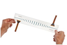
Process description : screen printing / slot die coating
Performances : large spectrum, high EQE, low dark current, large dynamic range, low power consumption, low temperature variation, benchmark vs silicon
The differentiating factors :
Printed photodetectors and image sensors offer similar performances to silicon (even better on some specific parameters) and open doors for new product development and innovation in different aspects :
. Cost optimization : thanks to fully printed manufacturing process (by deposition of liquid materials at air ambient and temperature ambient conditions), ISORG technology offers cost optimized process versus traditional silicon technologies, especially for larger area sensors (such as for X ray industry).
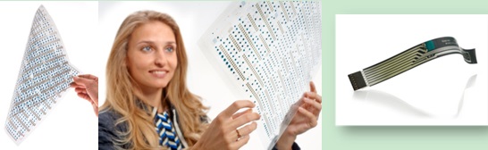
ISORG will offer image sensors of dimensions up to 60cm x 60cm.
. Mechanical robustness : replacement of glass substrate by a plastic substrate enables high resistance to shock for portable products for easier product manufacturing and robust usages, in particular for the industrial market.
. Mechanical integration : thanks to their unique properties, thin, light and flexible, these sensors open doors for innovative product design, in particular for wearable products such as smart watches. These sensors can be easily integrated in final products such as adhesive strips for retrofit of existing industrial equipments for Industrial Internet-Of-Things and connected objects : ISORG has started collaborative programs for optical sensors for process control for pharmacy industry.
ISORG has also developed solutions for co-integration of plastic electronics (plastic sensors, plastic foils) with traditional electronics (integrated circuits, LEDs) for system-on-foil integration.
. Innovative optical sensor design : thanks to their capability of flexibility and conformability, these sensors enable creation of very innovative optical sensors with curved surfaces for 3D image capture, for markets such as medical X ray or industrial X ray (tube inspection).
Screen printing process enables also fast and cost effective design of large area photodiode with specific dimensions and forms factors (thanks to low cost masks)
. Optical performances : organic image sensors offer high opto-electronics performances with low variation of dark current vs temperature and high EQE (External Quantum Efficiency) for Near Infra Red band.
Typical functionalities :
These new sensors are typically for scanner functionalities for image capture in direct contact or operation at short distance. They do not require any lenses.
Typical functionalities developed for photodiode products are :
Proximity detection and gesture detection for touchless HMI (Human Machine Interface)
Object detection
Angular position detection device
Position Sensing Device (laser detection)
Usage of traditional CMOS camera has limitations of physical dimensions to operate (ie minimum distance of camera for focalization) and usage of fragile optics, which means bulky and stationary equipment, such as biometrics scanners (airport control), bar code readers or diagnostics equipments. It is highly desirable for these industries to use innovative plastic electronics technology to develop portable and robust devices to replac existing equipments based on CMOS cameras. We can think of future tablet products integrating display and backside a scanning surface for fingerprint sensing, bar code reading or document scanning.
Typical functionalities developedfor image sensor productsare :
X ray scanner : large image sensor positioned in direct contact with scintillator which converts X ray signal into visible light.

Scanning surface for biometrics : large image sensor for fingerprint scanning (multiple fingers) or vein detection (with near infra-red light going through the skin) for fake finger detection
Photonic array integrated in display for touchless or 3D interaction
Scanning surface for bar code reading / optical character recognition
Photonic array for diagnostics and microfluidics

Market and applications :
This new technology is positioned on high growth markets of medical equipment, industrial Internet-Of-Things (IoT), Connected Objects, Security and Wearable devices.
Photonic sensors for industry : innovative large area photodiodes were developed for angular position detection of object placed over the surface or laser spot detection over a large surface.
Photonic sensors / photonic arraysfor connected objects and HMI : it is highly desirable for connected objects to have intuitive and robust user interfaces. Optical detection enables proximity detection and user interaction without touching the surface, which prevents traces of fingers or contamination (for instance for hospital or clean room environment). Optical detection also enables robust usages with wet or greasy fingers and gloves (which limits usage of traditional tactile / touch screen solutions) for home appliances products (such as fridges) and industrial displays. Integration of photonic array in display also enables to transform standard LCD display into interactive display with revolutionary 3D interaction (for rich user experience with graphics for instance).
Photonic sensors for industrial IoT : ISORG has developed complete solutions for object detection for real time inventory control and logistics (as substitute solution to RFID or bar code reading). This solution can also address connected retail with innovative usages of customer interaction and big data analysis.
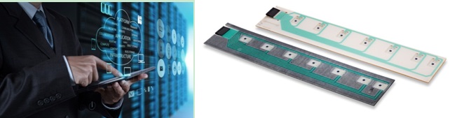

Image sensors for X ray digital imaging equipment (medical, industry and security) :
Organic technology will bring benefit of cost reduction, robustness (replacing glass substrate by plastic substrate), performances (high sensitivity, low variation vs temperature) and innovation (3D imaging with curved shape sensor).

Image sensors for Biometrics and Wearable Devices: for large area fingerprint scanning and vein recognition. Conformability and ultra thin profile of these sensors enables integration into wearable devices such as smart watches or smart bands.
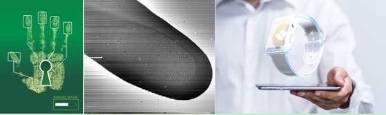
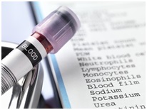
Image sensors for Health Sciences and Diagnostics
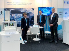 FISBA exhibits Customized Solutions for Minimally Invasive Medical Endoscopic Devices at COMPAMED in
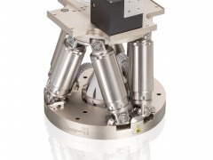 New Active Alignment System for the Coupling of Photonic Structures to Fiber Arrays
 A new industrial compression module by Amplitude
 Menhir Photonics Introduces the MENHIR-1550 The Industry's First Turnkey Femtosecond Laser of
 Shenzhen DNE Laser introduced new generation D-FAST cutting machine (12000 W)