AI is reshaping the field of photonic devices
source:Science Popularization China
keywords:
Time:2025-09-06
Source: Science Popularization China 6th August 2025
With the increasingly widespread application of big data, the Internet of Things and 5G systems, the demand for data transmission speed and capacity has sharply increased. The scale and computing efficiency of silicon-based electronic integrated chips are gradually approaching their physical limits. In contrast, photonic integrated chips, which use photons as information carriers, have the advantages of small size, high speed and high integration. They have developed rapidly in fields such as optical communication, quantum computing and quantum information processing.
We can compare photons to trains, and photon devices to train tracks and railway stations. The transmission and processing of photons in a photonic chip are like trains running on tracks and exchanging passengers (processing signals) at railway stations.
Waveguide is one of the most fundamental units in photonic chip devices, and its main function is to guide light along a specific path. The waveguide in photonic devices is similar to the common optical fiber we see, which can effectively confine light. In addition, various common optical functional devices can be fabricated using waveguides. For example, Figure 1a shows a directional coupler (DC), which is usually a photonic device composed of two waveguides. When light is transmitted in one of the waveguides, under certain specific conditions, the light is not completely confined within the waveguide, and a portion of it adheres to the outer surface of the waveguide (the evanescent field effect of electromagnetic waves). If the other waveguide is placed very close to this one, then this light can enter the other waveguide (that is, the coupling effect). Generally, the transmission of light signals between the two waveguides has a clear directionality, so this structure is called a directional coupler. By analyzing and processing the light signal in the second waveguide, specific functions can be achieved. The photonic device shown in the red dashed area of Figure 1b is called a Mach-Zehnder interferometer (MZI), which is also composed of two waveguides. However, the light in these two waveguides is input from the same end. The difference is that in this structure, by modulating the lower waveguide (usually by applying electricity), the phase of the transmitted light can be changed using the electro-optic effect (changing the refractive index), creating a phase difference between the upper and lower light beams, and thus generating interference to adjust the intensity of the light signal at the output port. It is widely used in phase modulation, optical intensity modulation, and optical polarization modulation, among other fields.
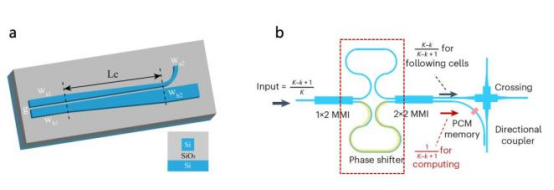
Figure 1: Several common photonic devices a directional coupler [1]; b Mach-Zehnder interferometer [2]
metasurfaces are another type of waveguide device, composed of nanostructure units arranged in a two-dimensional plane. Each unit functions like a miniature "optical antenna", capable of precisely regulating the phase, amplitude, and polarization state of light at the nanoscale. Through ingenious design of these structures, scientists can make light refract, reflect, focus, or even change color, brightness, or propagation direction in a pre-determined manner, as if equipping light with a "conductor's baton". For instance, in 2011, the Capasso team from the United States proposed a V-shaped antenna metasurface (Figure 2a), which can achieve abnormal deflection of electromagnetic wave transmission (Figure 2b, where the blue segments represent normal reflection and refraction paths, and the red segments represent abnormal reflection and refraction paths).

Figure 2: metasurface structure based on V-shaped antenna structure [3]
Among these photonic devices, the geometric parameters of the structure and external control parameters, such as waveguide width, coupling region length, spacing between waveguides, and intensity of the applied electrical signal, all result in different functions. When designing such photonic devices, it is necessary to identify specific parameters based on the desired function. Therefore, the structural design of photonic devices is particularly important.
The design of individual devices like waveguides is relatively easier. By adjusting a few parameters, such as the geometric dimensions and material types of the waveguide, the desired functions can often be achieved. However, when these photonic devices are integrated into photonic chips, for instance, a metasurface structure consists of multiple basic device units, and the relative angles, distances, and sizes between different basic units will affect their coupling and interaction, further increasing the design difficulty.
To reduce processing costs, it is necessary to rely on computer technology to conduct simulation and emulation before processing the devices, which can lower experimental costs and facilitate the design of more complex functional structures. For instance, commonly used numerical simulation methods include the Finite-Difference Time-Domain (FDTD) and the Finite Element Method (FEM).
Although such numerical simulation methods have been widely applied in the design of photonic devices, they still have certain limitations. Take FDTD as an example. During the simulation, the area to be simulated is first divided into extremely small grids, and the light propagation process is divided into countless extremely short instants. Then, according to the propagation law of light (Maxwell's equations), the light field of each grid at different times is calculated one by one. Finally, by piecing together these results, the complete process of light transmission in the device can be obtained. Due to the inherent characteristics of the FDTD numerical method, when simulating optical devices, the grid size of a single calculation area must be smaller than the wavelength. This ultra-high resolution requirement makes traditional methods inadequate when simulating large-scale photonic devices.
Furthermore, when designing and implementing a photonic device with a specific function, designers can usually only adjust certain specific parameters, such as the length of the coupling region and the width of the waveguide. However, there are many factors that actually affect the performance of the device. This method of adjusting specific structural parameters greatly limits the design freedom. For more complex devices, it is often necessary to try a large number of different parameter combinations to find the optimal solution. The computational cost and time increase exponentially with the number of parameters. Sometimes, it takes several days or even weeks to complete the design of a photonic device that meets the usage requirements. For example, if one wants to simulate the influence of the waveguide's geometric dimensions on light transmission, three parameters need to be considered: the width, height, and length of the waveguide. If the variation range of each parameter is from 11 μm to 20 μm and the step size is 1 μm, there are 10 possibilities for each dimension, and 1000 possibilities for the three dimensions. This means that the computer needs to perform 1000 calculations to complete the simulation. Therefore, the size of the photonic devices that can be designed using the above method is usually only at the hundred-micron scale.
In conclusion, traditional methods not only consume a large amount of computing resources but also have limitations in terms of integration.
In recent years, the rapid development of Artificial Intelligence (AI) technology has provided new opportunities for scientific research. In 2024, both the Nobel Prize in Physics and Chemistry were awarded to scientists in the field of AI. Machine learning, especially deep learning, has been widely applied in the efficient design of microstructures and structural optimization, significantly reducing the design time of microstructures and also providing new technical means for the design of large-scale structures.
So, how does AI manage to do that?
Firstly, AI collects a large amount of data on specific optical structures and their corresponding optical properties, and uses this data to train deep learning models. This is similar to us first allowing the model to learn a "dictionary" (referred to as the forward model network), matching structural parameters with optical performance. After training, the model becomes an experienced design expert. Then, when specific functional requirements are input into the model, it will search for similar structures in the dictionary. Of course, this structure still cannot meet the requirements and further optimization of the initial design is needed (referred to as the inverse design model network).
To achieve the precise mapping of "structure → performance" by the forward model network and the reverse optimization from "function → structure" by the reverse design model network, scientists have proposed many optimization methods. Among these methods, the gradient descent algorithm, due to its simplicity and efficiency, is currently the most widely used one.
This solution is like when we are on the top of a mountain looking for the shortest path to the valley. When you are standing on the top of the mountain, you don't know the best path yet, only a rough direction. If it were you, what would you do?
When going downhill, you need to determine the direction of descent based on the current slope. The usual approach is to keep moving in the direction of the slope's descent, always heading towards the steepest direction, which will allow you to quickly approach the valley (Figure 3).

Figure 3: Schematic Diagram of Finding the Shortest Path Down the Mountain [4]
At this point, you may wonder: If you walk in the direction of the steepest gradient, will you definitely reach the valley?
In fact, if while walking, one encounters a small depression and no matter which direction one takes the next step, it is all in the direction of increasing gradient, the model would think this is a valley, but in reality, it is not.
This situation of encountering a "false valley" causes the AI to get stuck in a "local minimum" and unable to reach the "global minimum". To avoid this problem, methods such as adjusting the step size and introducing random disturbances can be used to help the AI quickly escape the small depression and find the "global minimum", thus reaching the valley.
When designing photonic devices, it is usually based on existing knowledge or experience to design some possible device structures. At this time, we do not know which structural parameters are the best, and the light transmission efficiency is still relatively low and the loss is still relatively large. The rate of change of the performance of the current structure (such as transmission efficiency, light loss, integration, etc.) with respect to each design parameter (such as waveguide width, material refractive index, etc.) is the "gradient", which is equivalent to the "slope" when going downhill. AI calculates the influence of different parameters on the final performance to obtain the "gradient". For example, starting from point A, by finding the largest "gradient" nearby and moving along this direction, you can reach point B, thereby reducing the value of the objective function (such as the loss function) (Figure 4). This is like you judging the direction of the next step in the mountains based on the slope. Repeat this step, gradually adjust the model parameters, and make the objective function reach the minimum value. Eventually, you can reach the lowest point C. This process helps AI know how to adjust the design parameters so that the performance of the photonic device gradually improves.

Figure 4: Schematic Diagram of Gradient Descent Algorithm [4]
Similarly, when AI designs photonic devices, the learning rate determines the pace of each adjustment to the design parameters. If the learning rate is too large, the model may overshoot and end up with a poor design due to excessive adjustments; if it is too small, the model will converge slowly, be inefficient, or get stuck in a "local minimum".
In summary, AI continuously optimizes within a vast design space. Through constant adjustments and optimizations, it eventually finds the best parameters. At this point, AI is like you successfully reaching the lowest point in the valley from the mountain top, identifying the most suitable photonic device structure that maximizes its performance. With this method, we can quickly design corresponding structures based on our needs, significantly reducing design time and enhancing accuracy. It can even create many structures that are beyond human imagination.
We take the metasurface structure as an example to explain how AI designs photonic structures. Figure 5 shows a resonant metasurface structure with a scale smaller than the wavelength and a high quality factor [5]. Similar to the metasurface structure in Figure 2, this metasurface structure is also a two-dimensional planar structure composed of many basic unit structures (the blue structures in Figure 5). Each basic unit consists of two identical silicon nanorods. A high quality factor means that light can be strongly "trapped" in these structures without radiating outward, allowing photons to stay for a longer time and greatly enhancing the interaction efficiency between light and materials. By taking advantage of the resonant characteristics of this structure, it can be used in optical sensing, nonlinear optics, and other fields. Due to the fact that even slight changes in the structure parameters can significantly affect the characteristics of the resonant spectrum, traditional design methods simulate the corresponding performance by continuously adjusting the structure parameters to achieve the desired function. However, this approach can only optimize one or two parameters simultaneously, and the range and precision of parameter optimization are limited. In reality, the performance control requires simultaneous optimization of multiple variables such as material properties and geometric characteristics. Therefore, traditional methods have limited control over the linewidth and width of the resonant spectrum and are very time-consuming.
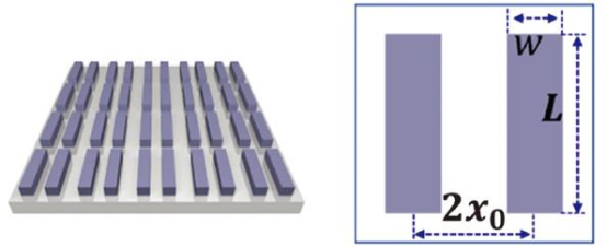
Figure 5: Schematic diagram of a silicon nanorod metasurface structure [5]
To enhance the efficiency of structural design, scientists first connected a pretrained forward model network and an inverse-design model network in series using an artificial neural network model (neural networks are core technology models of artificial intelligence, inspired by the neural networks in the human brain) (Figure 6). Then, an open-source neural network library was used to train the forward model network to learn the mapping relationship ("dictionary") between the parameters of the metasurface structure (y1, y2... on the right side of Figure 6) and the transmission spectrum (x1, x2... on the right side of Figure 6). Next, the output of the inverse-design model network (y1, y2... on the left side of Figure 6) was connected to the trained forward model network. By learning this "dictionary", it was possible to know how to find the appropriate metasurface structure parameters based on the target optical response (x1, x2... on the right side of Figure 6). That is, this "dictionary" was used to assist the inverse-design model network in predicting the structure parameters from the optical response. Finally, the inverse-design model network predicted the structure parameters based on the optical target and updated its own parameters by comparing the error between the output of the forward network and the target response to minimize the difference between the input and predicted results (i.e., the gradient descent algorithm), thereby predicting the metasurface structure parameters that meet the conditions and achieving efficient and accurate metasurface design.

Figure 6: The TN model architecture [5] composed of a reverse design model network and a pre-trained forward model network, where X represents the input and output, i.e., the transmission spectrum data, and Y represents the output of the intermediate layer, corresponding to the structural parameters.
By inputting the transmission spectrum parameters of the metasurface structure: the working wavelength λ = 1500 nm, the linewidth (half-width of the resonance peak) Δλ = 5 nm, and the shape factor (used to describe the asymmetry of the spectrum) q = 0.5 (the corresponding spectrum is shown as the black dashed line in Figure 7), ultimately, with the fixed basic unit period D = 900 nm and the thickness of the nanorods 150 nm, the neural network model designed the nanorod width w = 316 nm, length L = 580 nm, and the spacing between the two nanorods in each basic unit 2x0 = 378 nm. The transmission spectrum corresponding to this structure is shown as the red solid line in Figure 7. It can be seen that the spectrum of the predicted structure by the model is very close to the input spectrum (the target result).

Figure 7: Comparison of the input transmission spectrum (black dashed line) and the transmission spectrum of the structure predicted by the neural network model (red solid line) [5]
If traditional numerical simulation methods are employed, professional computers are required and it takes at least seconds to complete. based on this method, the optical metasurface structure design was accomplished within 0.05 seconds using an ordinary computer (Intel(R) Core(TM) i7-4770 CPU @ 3.40 GHz, RAM: 16.0 GB), significantly enhancing the design efficiency.
In addition to assisting researchers in photonics structure design, researchers have discovered that photonic chips can also be used to implement the photonic structure of neural networks. Compared with traditional electronic chips, photonic neural networks have obvious advantages in computing speed and power consumption. For example, in 2022, Firooz et al. implemented a system that uses an on-chip photonic deep neural network to recognize handwritten letters (Figure 8). The research team input the light intensity information of each pixel of the handwritten letter image into the system through a grating coupler. By weighting the input signal (Optical attenuator part, optical attenuator), the light then enters the photodetector (PD part) to complete the addition operation, and then the microring resonator (Optical modulator part) performs nonlinear transformation (complex feature extraction), and finally the optical signal is transmitted to the next layer of the neural network (Neuron optical output).

Figure 8: Handwritten letter recognition using photonic chips [6]
These achievements demonstrate the huge application potential of artificial intelligence in photonic devices, laying the foundation for the development of a new generation of efficient and feature-rich photonic devices. We believe that with the rapid development of artificial intelligence technology, a huge technological revolution will come to the field of micro-nano photonic device design and application. In the near future, the electronic devices we use now may all become a world of photons.
We can boldly imagine what the future world will be like.
Perhaps by then, thanks to the advantages of photons in high-speed information transmission and processing, optical quantum computers will enter every household just like today's smart phones.
References
[1] WANG Q, HE Y, WANG H, et al. On-chip mode division (de)multiplexer for multi-band operation [J]. Opt. Express, 2022, 30(13): 22779-22787.
[2] DONG B, AGGARWAL S, ZHOU W, et al. Higher-dimensional processing using a photonic tensor core with continuous-time data [J]. Nat. Photon., 2023, 17(12): 1080-1088.
[3] YU N, GENEVET P, KATS M A, et al. Light Propagation with Phase Discontinuities: Generalized Laws of Reflection and Refraction [J]. Science, 2011, 334(6054): 333-337.
[4] 王东,马少平. 图解人工智能 [M]. 北京: 清华大学出版社, 2023.
[5] XU L, RAHMANI M, MA Y, et al. Enhanced light–matter interactions in dielectric nanostructures via machine-learning approach [J]. Advanced Photonics, 2020, 2(02): 026003.
[6] ASHTIANI F, GEERS A J, AFLATOUNI F. An on-chip photonic deep neural network for image classification [J]. Nature, 2022, 606(7914): 501-506.
 56 Benchmarks Honored: 9th Secret Light Awards Highlights China Laser Chain Innovation
 Laser Intelligence, Photonics Future: XZQ 2026 WLMC Concludes Successfully
 Laser Giants' AI Bet: Decoding Earnings to Find the Next Winner
 Orders Reign Supreme: Laser Firms' Battle—$10B Backlogs vs. Overseas Breakouts
 Q1 Earnings Released: A Tale of Two Strategies Among the World's Four Largest Laser Companies
 HSG Laser's He Hongming: Innovation Drives Laser Manufacturing Future
 Xi Jingyu from Mingyu Technology: Carving the Future of Hometown Industries with Laser
 Qiming Photonics: Nobel-Powered "Optical Engine" for the Computing Age
 Chen Kangkang of Anyang Laser: The "Hard Tech Long March" Behind a Single Optical Fiber
 Exclusive Interview with Academician Gu Bo: Escaping the Involution Trap in the Laser Industry