Finetech: High Precision Die Bonders for Advanced Optoelectronic Applications
source:laserfair.com
Time:2016-07-06
German equipment manufacturer Finetech presents highlights of the acclaimed FINEPLACER® product line at CIOE 2016 in Shenzhen, China, September 6-9, 2016, booth #1A13-16.
As a long-term technology partner for high-precision die packaging and advanced optoelectronic applications, Finetech has profound experience in the development of manual to fully-automatic sub-micron die bonders for R&D, prototyping and production.
All FINEPLACER® die bonders have been designed to support a particular wide range of applications at chip and wafer level. This includes low/high power laser bar and diode bonding with Indium or Au/Sn, bonding of single and array VCSEL/photo diodes (gluing, curing), µLED bonding, the assembly of lenses, mirrors or filters, the multi-stage assembly of Transmitter Optical Sub-Assemblies and Receiver Optical Sub-Assemblies or opto electro mechanical systems (i.e. MEMS/MOEMS), and many more.
FINEPLACER® systems provide optimal process environments for each application. Their modular system architecture allows highly customized machine configurations. New processes and technologies can be easily retrofitted with extension modules.
.jpg)
FINEPLACER® lambda – 0.7 µm optical resolution and technological flexibility
The sub-micron Opto-Bonder® FINEPLACER® lambda offers outstanding optical resolution up to 0.7 µm. Depending on application requirements, a smart optics clamping system allows easy retrofitting of different available optics to switch between fields of view and optical resolutions.
The FINEPLACER® lambda is the ideal fit for precision die attach and advanced packaging in photonics and opto-electronic applications, whenever maximum technological versatility and fast process implementation is required (i.e. for R&D, universities, prototyping).
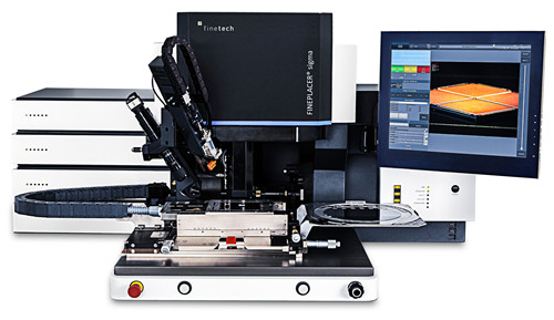
FINEPLACER® sigma - Sub-micron Chip Packaging on Wafer Level
The FINEPLACER® sigma is the first bonding platform to combine sub-micron placement accuracy with a working area suitable for 300 mm wafer substrates and bond forces up to 1000N.
This combination of features makes the FINEPLACER® sigma well-suited for Wafer Level Packaging (FOWLP, W2W, C2W), high-precision 2.5D and 3D IC packaging, MEMS/MOEMS/IR/image sensor assembly/Focal Plane Arrays and all kinds of high I/O count applications.
The cutting-edge FPXvisionTM Vision Alignment System provides maximum optical resolution at all magnification levels. Real-time optimized camera images helps representing smallest structures even of large components and substrates. Optical pattern recognition gives precise position feedback for a software-assisted verified alignment process.
The FINEPLACER® sigma supports advanced bonding technologies such as laser-assisted die bonding, precision vacuum soldering, sintering or metal diffusion bonding (Cu/Cu) for R&D and prototyping environments.
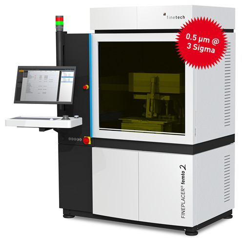
FINEPLACER®femto 2 – Automatic Sub Micron Bonder
The FINEPLACER®femto 2 is a fully-automated die bonder with a placement accuracy of 0.5 µm @ 3 Sigma. A complete machine enclosure allows demanding applications in a controlled environment. Fully protected from external influences, the system stands for highly stable assembly processes with the focus on maximum yield.
The new generation of the femto platform comes with the FPXvisionTM Vision Alignment System, refined pattern recognition and fully revamped operating software to support a streamlined process development.
The FINEPLACER®femto 2 is the perfect tool to migrate applications from product development to the automated production stage. It covers the entire workflow of inspection, characterization, packaging, final test and qualification in semiconductor, communications, medical and sensor technologies.
 2026 China Laser Leadership Summit Opens in Shanghai, Leaders Talk Laser-Intelligence Integration
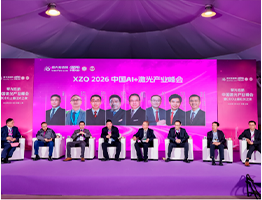 8 Laser Leaders Debate Laser-AI Integration & Two-Way Empowerment at Shanghai Summit
 10 New Laser Startups Emerge; Giants Like Han's Laser Nurture New Players for Future Race
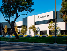 Lumentum Expands U.S. Chip Manufacturing to Supply AI Data Center Core Lasers
 Surges Sharply at Opening! Han's CNC Successfully Listed on the Hong Kong Stock Exchange
 Qiming Photonics: Nobel-Powered "Optical Engine" for the Computing Age
 Chen Kangkang of Anyang Laser: The "Hard Tech Long March" Behind a Single Optical Fiber
 Exclusive Interview with Academician Gu Bo: Escaping the Involution Trap in the Laser Industry
 Li Qi from Sichuang Laser: Pioneering High-Power Laser Tech for New Cross-Industry Use Cases
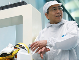 Awardee Chen Weibiao Pushes Space Laser Tech to Build China's Aerospace Leadership