
Laser Diodes: The power of brilliance -- the past and future of high-power semiconductor lasers
source:Laser Focus World
release:Nick
keywords: semiconductor lasers Laser Diodes
Time:2018-01-24
Traditionally, economists have viewed technological progress as an incremental process. Recently, greater focus has been placed on the role of disruptive innovations that introduce a discontinuity. These innovations have been called general-purpose technologies (GPTs), and are "deep new ideas or techniques that have the potential for important impacts on many sectors of the economy."[1] Clear examples of GPTs are the steam engine, electricity, and the integrated circuit.
General-purpose technologies typically take decades to develop and even longer to lead to productivity improvements. They are usually not well understood at first and there is a subsequent long lag in productive adoption, even after the technology is commercialized. The integrated circuit is a good case study. While the transistor was first demonstrated early in the 20th century, broad commercialization occurred much later.
Gordon Moore’s short paper in 1965 predicted that semiconductors would improve at a rapid rate, allowing a "proliferation of electronics, pushing this science into many new areas."[2] Despite his bold and surprisingly accurate predictions, it took decades of continued improvement before the realization of productivity improvements and economic growth.
Similarly, there is limited understanding of the dramatic improvement in high-power semiconductor lasers. The conversion of electrons into laser light through a semiconductor was first demonstrated in 1962, and subsequently, there have been a wide range of complementary advancements that have driven dramatic improvements in the conversion of electrons into highly productive laser light. These improvements have supported important applications ranging from optical storage to optical networks to a broad range of industrial applications.
Looking back at these advancements and their cumulative improvements highlights the potential for even larger and more ubiquitous effects on many sectors of the economy. Indeed, as high-power semiconductor lasers continue to improve, the range of important applications will likely accelerate and profoundly shape economic growth.
On the morning of Sunday, September 16, 1962, Robert Hall’s team at General Electric Research Labs demonstrated infrared emission from a gallium arsenide (GaAs) semiconductor with a "strange" interference pattern implying coherent laser light—the first semiconductor laser was born.3 Hall originally thought that a semiconductor laser was a "long shot" because light-emitting diodes at the time had very low efficiency. He was also skeptical because the existing lasers, which had only been demonstrated two years earlier, required "fancy mirrors."[2]
In the summer of 1962, Hall said he was "shaken up" by a paper that showed much higher efficiency GaAs light emitting diodes from MIT Lincoln Labs.[3] He went back to General Electric and recalled that he was fortunate to have some good quality GaAs material to test and he drew on his experience as an amateur astronomer to develop an approach to polish the edges of the GaAs chip to form a cavity.[4]
Hall’s successful demonstration was based on his design where the radiation bounced back and forth in the plane of the junction and not perpendicular to it. He modestly suggested that no one had "stumbled onto this idea before." Indeed, Hall’s design was a fortunate coincidence of nature that semiconductor materials that form waveguides also have the property of simultaneously confining bipolar carriers. Otherwise, semiconductor lasers would not be possible. By using dissimilar semiconductor materials, a slab waveguide could be formed to overlap the photons with the carriers.
These initial demonstrations at General Electric were a fundamental breakthrough. However, these lasers were far from practical devices and to fulfill the promise of high-power semiconductor lasers, a confluence of disparate technologies had to be realized. Key technology innovations began with advances in the understanding of direct bandgap semiconductor materials and crystal growth technologies.
Later developments included the invention of double heterostructure lasers and the subsequent development of quantum well lasers. Critical to further enhance these core technologies were the improvement in efficiency and the development of facet passivation, heatsinking, and packaging technologies.[5]
These innovations over the past several decades have resulted in cumulative improvements that have been surprising. In particular, the improvements in brilliance have been extraordinary.[6] In 1985, a state-of-the-art, high-power semiconductor laser could couple a mere 100 mW of power into a 105 μm core diameter fiber. State-of-the-art high-power semiconductor lasers can now produce over 250 W into a 105 μm fiber with a single wavelength—an exponential improvement by a factor of 10 every eight years.
Moore speculated about "cramming more components onto integrated circuits"—subsequently, the number of transistors per chip have increased by a factor of 10 every seven years. Coincidentally, high-power semiconductor lasers have been cramming more photons into fiber at a similar exponential rate (see Fig. 1).

FIGURE 1. High-power semiconductor laser brilliance and Moore’s Law are compared.
Improvements in the brilliance of high-power semiconductor lasers have been the result of a wide range of unforeseen technology advancements. While new innovations are required to continue this trend, there is reason to believe that innovation in semiconductor laser technology is far from exhausted. Well-understood physics can further enhance the performance of semiconductor lasers with continued engineering development.
For example, quantum dot gain media promise significant increases in efficiency over current quantum well devices. Slow-axis brightness offers the potential for improvement by yet another order of magnitude. Novel packaging materials with improved heat spreading and expansion-matching will provide the enhancements necessary for continued power scaling and simplified thermal management. These critical developments will support the roadmap for high-power semiconductor lasers in the coming decades.
High-power semiconductor laser improvements have enabled growth in downstream laser technologies where the semiconductor laser is used to excite (pump) a doped crystal (diode-pumped solid-state lasers) or doped fiber (fiber lasers).
While semiconductor lasers offer a highly efficient, small, low cost source of laser energy, there are two key limitations: they do not store energy and their brightness is limited. Essentially two lasers are required to be useful for many applications; one to convert electricity to laser emission, followed by another to enhance the brightness of that emission.
Diode-pumped solid-state lasers. In the late 1980s, the use of semiconductor lasers to pump solid-state lasers started to gain considerable interest for commercial deployment. Diode-pumped solid-state lasers (DPSSLs) dramatically reduced the size and complexity of the thermal management systems (primarily recirculating chillers) and gain blocks that historically had incorporated arc lamps to pump the solid-state laser crystal.
Semiconductor laser wavelengths were chosen based on their overlap with spectral absorption features of the solid-state laser gain medium, significantly reducing the heat load when compared to the broadband emission spectrum of arc lamps. Given the popularity of neodymium-based lasers emitting at 1064 nm, a pump wavelength of 808 nm became the highest volume wavelength in production for semiconductor lasers for over 20 years.
As the brightness of multimode semiconductor lasers improved and the ability to stabilize narrow emission linewidths with volume Bragg gratings (VBGs) became possible in the mid-2000s, a second generation of improved diode pumping efficiency was realized. Weaker and spectrally narrow absorption features around 880 nm attracted great interest for high-brightness pump diodes that could be spectrally stabilized. These higher performance lasers enabled direct pumping of the upper laser level 4F3/2 in neodymium, reducing the quantum defect, and thus improving fundamental mode extraction at higher average powers that would otherwise be limited by thermal lensing.
By the early 2010s, we witnessed a trend of significant power scaling of single transverse mode 1064 nm lasers and their associated family of frequency converted lasers operating at visible and ultraviolet wavelengths. Given the long upper-state lifetime of Nd:YAG and Nd:YVO4, Q-switched operation of these DPSSLs offer high pulse energies and peak powers well suited for ablative material processing and high-precision micromachining applications.
Fiber lasers. Fiber lasers offer a cost-effective way to convert the brilliance of a high-power semiconductor laser. While wavelength-multiplexing optics can convert a relatively low-brightness semiconductor laser to a brighter one, this comes at the expense of increased spectral width and optomechanical complexity. Fiber lasers have proven particularly effective at brilliance conversion.
As an example, compare the following best-in-class laser where ~5 kW of 976 nm pump power from 400 μm and 0.46 NA fiber (95 mm-mrad of beam quality), which is equivalent to 0.55 W/(mm-mrad)2 of pump brilliance. That pump light gets converted by a fiber laser to ~4 kW of 1064 nm from a 20 μm and 0.06 NA beam, which has a brilliance of 11,098 W/(mm-mrad). The brilliance enhancement provided by the fiber laser is >20,000x—or over four orders of magnitude!
Double-clad fibers introduced in the 1990s use a single-mode core surrounded by a multimode cladding to enable efficient launching of higher-power, lower-cost multimode semiconductor pump lasers into fiber, thus creating a more economical way to convert high-power semiconductor lasers to a brighter source. For fiber doped with ytterbium (Yb), the pump excites a broad absorption feature centered at 915 nm or a narrower band around 976 nm. As the pump wavelength approaches the lasing wavelength of the fiber laser, the so-called quantum defect is reduced, maximizing efficiency and minimizing the amount of waste heat to be dissipated.
Both fiber lasers and diode-pumped solid-state lasers have relied on improvements in diode by laser brilliance. In general, as diode laser brilliance advances, so does the power scaling of the lasers they pump. Brilliance improvements in semiconductor lasers tend to promote more efficient brightness conversion.
As we look forward, both spatial and spectral brightness will become necessary for future systems that will enable low-quantum-defect pumping of narrow absorption features in solid-state lasers and dense wavelength multiplexing schemes for direct semiconductor laser applications.
The advancements in high-power semiconductor-based lasers have enabled numerous important applications. These lasers have both displaced older technologies and enabled new categories of products as high-power semiconductor lasers have improved exponentially in cost per bright watt.
With an improvement of cost and performance of over a factor of 10 every decade, high-power semiconductor lasers have disrupted markets in unforeseen ways. While it is difficult to precisely forecast future applications, it is instructive to look back over the last three decades to frame the possibilities in the next decade (see Fig. 2).
![FIGURE 2. High-power semico<em></em>nductor laser brilliance fuels applications (Normalized cost per bright watt*) [*Bright Watt = Brilliance (W/cm2 -sr)].](http://aemstatic-ww2.azureedge.net/content/dam/lfw/print-articles/2018/01/1801LFW_kee_f2.jpg)
FIGURE 2. High-power semiconductor laser brilliance fuels applications (Normalized cost per bright watt*) [*Bright Watt = Brilliance (W/cm2 -sr)].
1980s: Optical storage and initial niche applications. Optical storage was the first large application for semiconductor lasers. Soon after Hall’s initial demonstration of an infrared semiconductor laser, Nick Holonyak, also at General Electric, demonstrated the first visible red semiconductor laser. Twenty years later, the compact disc (CD) was introduced to the market and the optical storage market was launched.
Continued innovations in semiconductor laser technologies brought optical storage evolutions such as the digital versatile disc (DVD) and then the Blu-ray disc (BD). This was the first large market for semiconductor lasers, but the generally modest power levels limited other applications to relatively small niche markets such as thermal printing, medical applications, and select aerospace and defense applications.
1990s: Optical networking boom. In the 1990s, the semiconductor laser became the linchpin of communications networks. Semiconductor lasers were used to transmit signals over fiber optic networks, but the higher power single mode pump lasers used in optical amplifiers were critical to enable optical networks to economically scale and to truly support the growth in data over the Internet.[7]
The resulting telecom bubble was profound as exemplified by one of the initial pioneers in high power semiconductor lasers, Spectra Diode Labs (SDL). Established in 1983 as a joint venture by Spectra-Physics and Xerox, SDL went public in 1995, with a market capitalization of roughly $100 million. Five years later SDL was sold during the peak of the telecom boom to JDSU for over $40 billion–one of largest technology acquisitions in history. Soon after, the telecom industry went bust, destroying trillions of dollars in capital and is now viewed as perhaps the largest bubble in history.[8]
2000s: Laser as a tool. While the telecom bust was highly disruptive, the large investments made in high power semiconductor lasers set the stage for broader adoption. As both performance and cost improved, these lasers increasingly displaced legacy gas lasers or other sources of energy transfer in a broad variety of processes.
Semiconductor based lasers have become ubiquitous tools used in a wide range of applications. Industrial applications range from traditional manufacturing processes such as cutting and welding, to new advanced manufacturing techniques such as additive manufacturing for 3D printing metal parts. Microfabrication applications are even more diverse as key products such as smart phones have been made commercially viable by the precise power delivery of these lasers. Aerospace and defense applications span a wide range of mission-critical applications, and in the future will likely include next-generation directed energy systems.
More than 50 years ago, Moore did not posit a new fundamental law of physics, rather he noted the exponential improvement in integrated circuits that had originally been investigated over a decade earlier. His predictions continued to hold for decades and enabled a series of disruptive innovations that could not have been envisioned in 1965.
When Hall demonstrated the semiconductor laser, also over 50 years ago, he launched a technology revolution. As with Moore’s Law, no one could have predicted the subsequent exponential advances in the brilliance of high-power semiconductor lasers that have been enabled by a wide range of disparate innovations.
There is no fundamental law of physics governing these improvements, yet it is likely that continued technology advancements can sustain this exponential improvement in brilliance. This will continue the displacement of legacy technologies and will further change the way that things are made. Even more fundamental to economic growth, high-power semiconductor lasers will also change what things can be made.
1. P. A. David and G. Wright, Gavin, "General purpose technologies and surges in productivity: historical reflections on the future of the ICT revolution," The Economic Future in Historical Perspective, edited by P. A. David and M. Thomas, Oxford University Press for the British Academy (2003).
2. G. Moore, "Cramming more components onto integrated circuits," Electronics, 38, 8, 114 (Apr. 19, 1965).
3. R. N. Hall, G. E. Fenner, J. Kingsley, T. J. Soltys, and R. O. Carlson, Phys. Rev. Lett., 9, 366 (1962).
4. See https://youtu.be/3B1P9ERCaxg.
5. D. F. Welch, IEEE J. Select. Topics Quantum Electron., 6, 6 (Nov/Dec. 2000).
6. Brilliance or "Bright Watt," defined as (watt/cm2-sr) or watt/(mm-mrad)2.
7. See https://goo.gl/QmY88o.
8. "The great telecoms crash," The Economist (Jul. 18, 2002); see www.economist.com/node/1234886.
 FISBA exhibits Customized Solutions for Minimally Invasive Medical Endoscopic Devices at COMPAMED in
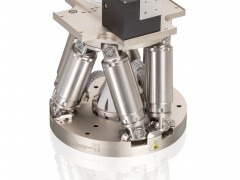 New Active Alignment System for the Coupling of Photonic Structures to Fiber Arrays
 A new industrial compression module by Amplitude
 Menhir Photonics Introduces the MENHIR-1550 The Industry's First Turnkey Femtosecond Laser of
 Shenzhen DNE Laser introduced new generation D-FAST cutting machine (12000 W)